InP HBT Transceivers
Electronic component and system design
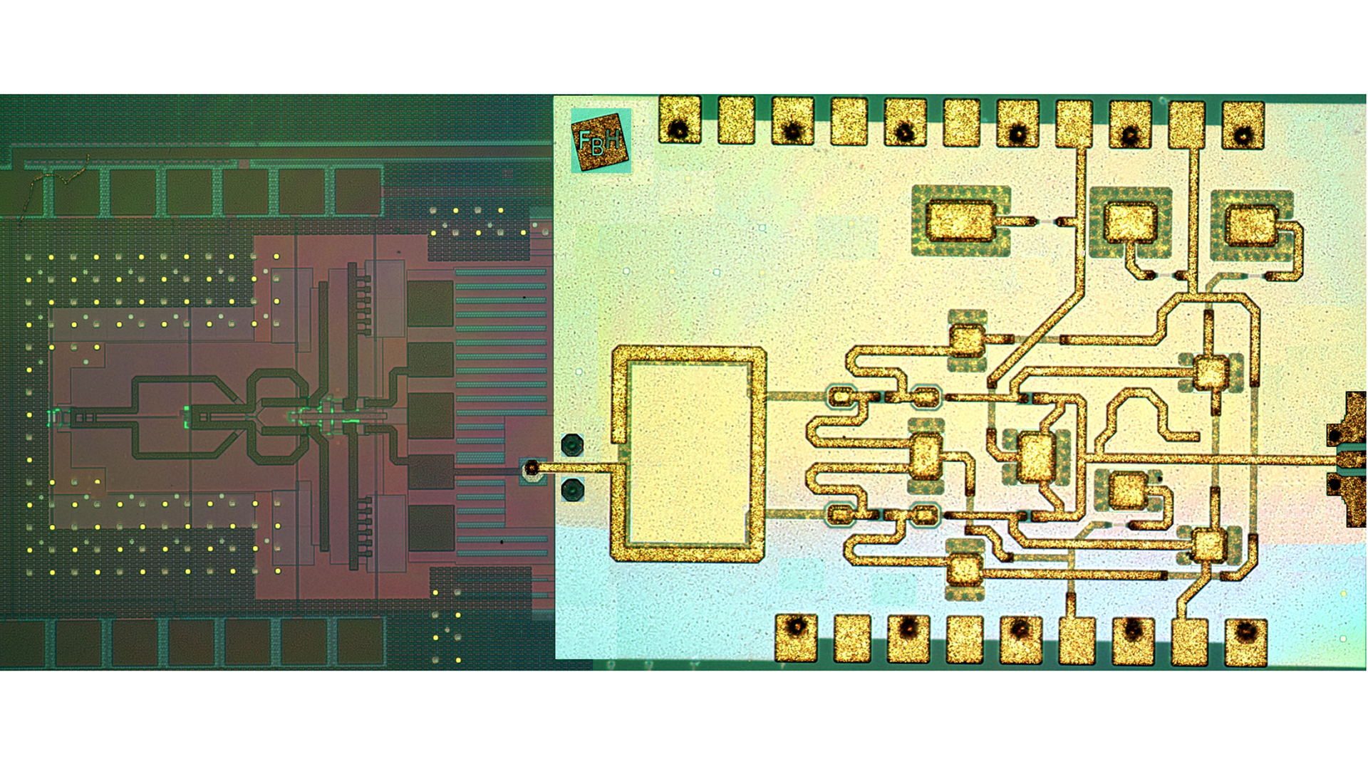
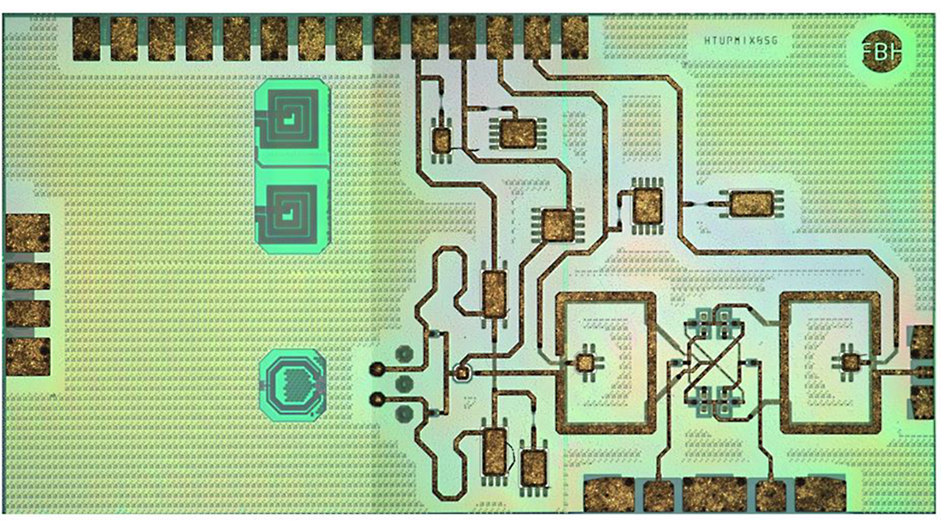
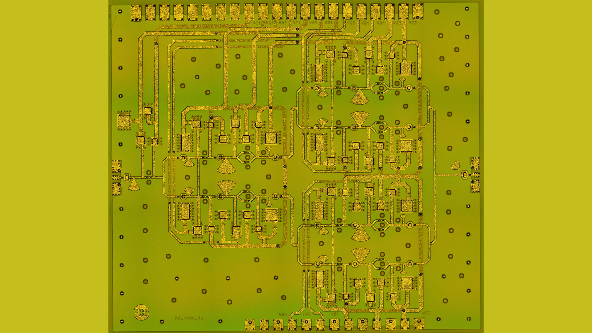
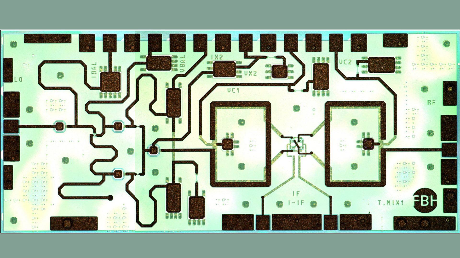
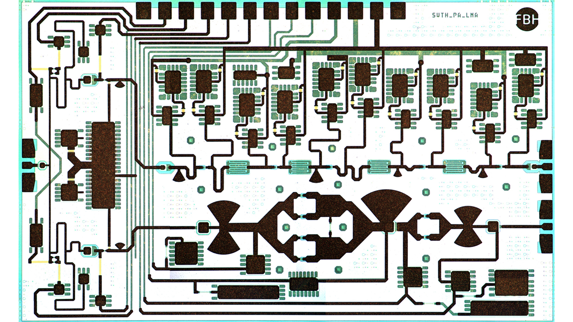
FBH has established a joint laboratory Goethe-Leibniz-Terahertz-Center with Goethe University Frankfurt and foundry activities with Leibniz-Institut für innovative Mikroelektronik (IHP). FBH operates an indium phosphide (InP) double heterojunction bipolar transistor (DHBT) transferred-substrate (TS) process and an InP-on-BiCMOS DHBT process. They reach cut-off frequencies around 500 GHz today and are being extended to yield over 700 GHz. We have demonstrated nonlinear active integrated circuits (MMIC) up to 300 GHz as building blocks for system-on-chip solutions, using heterogeneous integration with silicon and diamond materials.
MMIC design at FBH is based on a MMIC design kit with active and passive elements and proprietary large-signal HBT device models including thermal effects. InP HBT technology offers operation at voltages up to 3.5 V and high frequencies with excellent phase-noise properties. Therefore, we focus on signal generation and amplification circuits. Additionally, we have demonstrated flip-chip transitions up to 500 GHz.
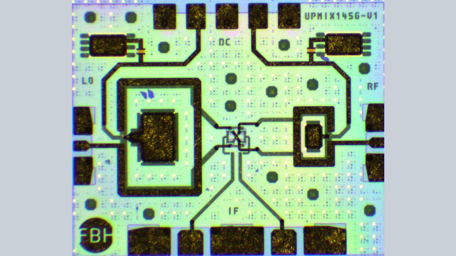
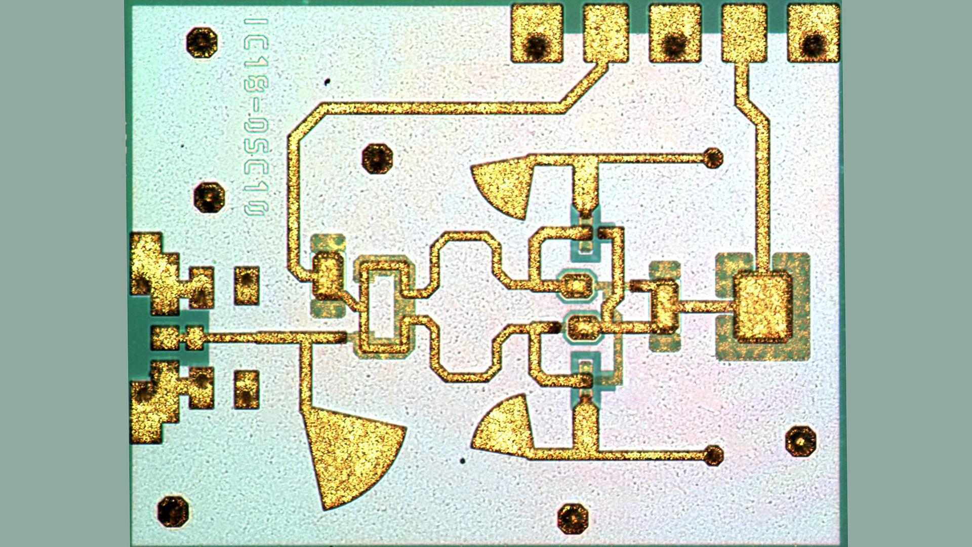
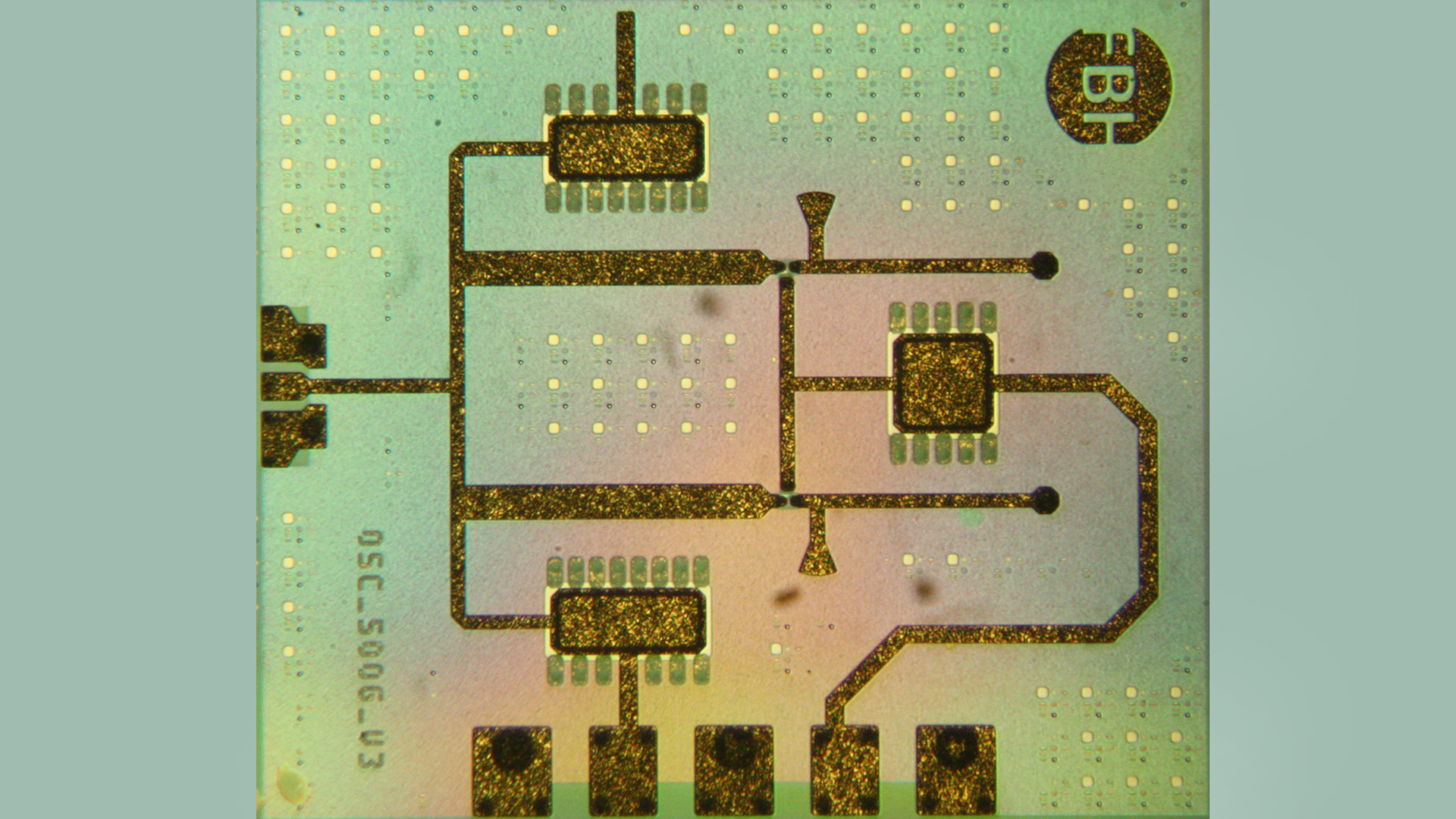
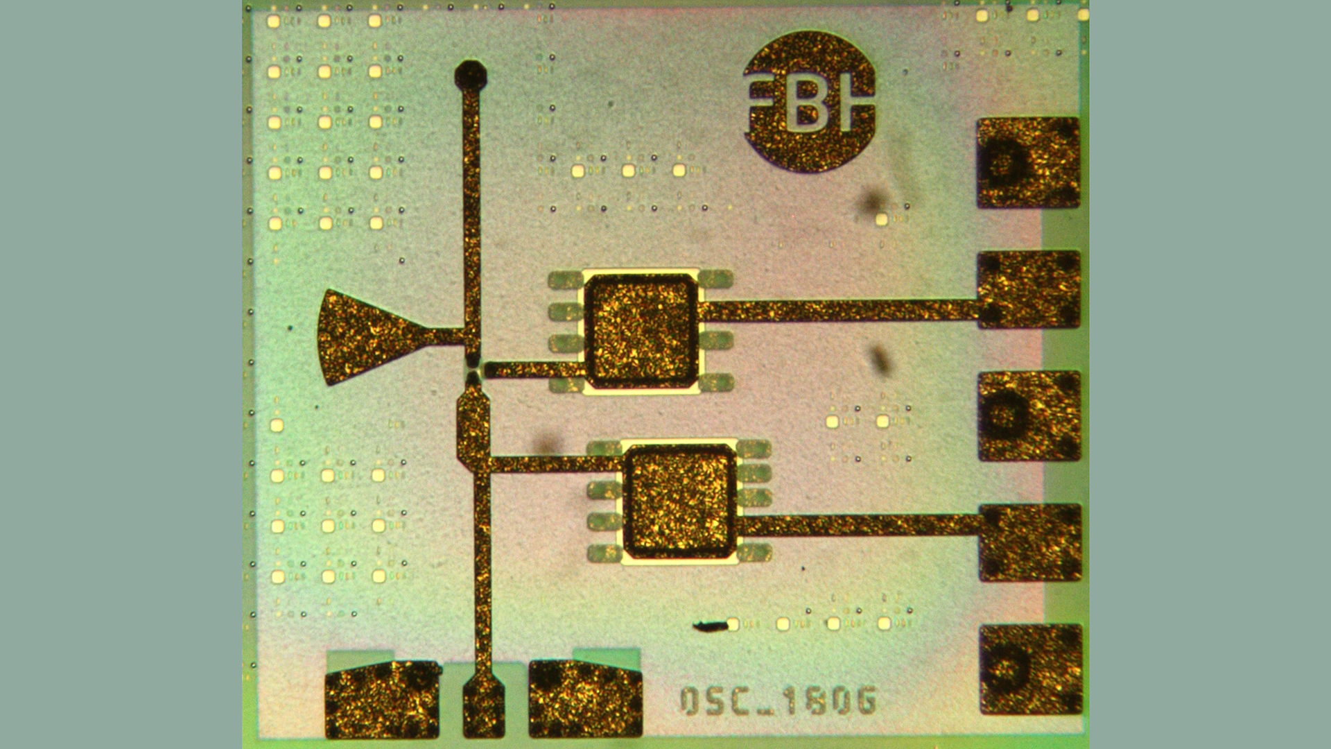
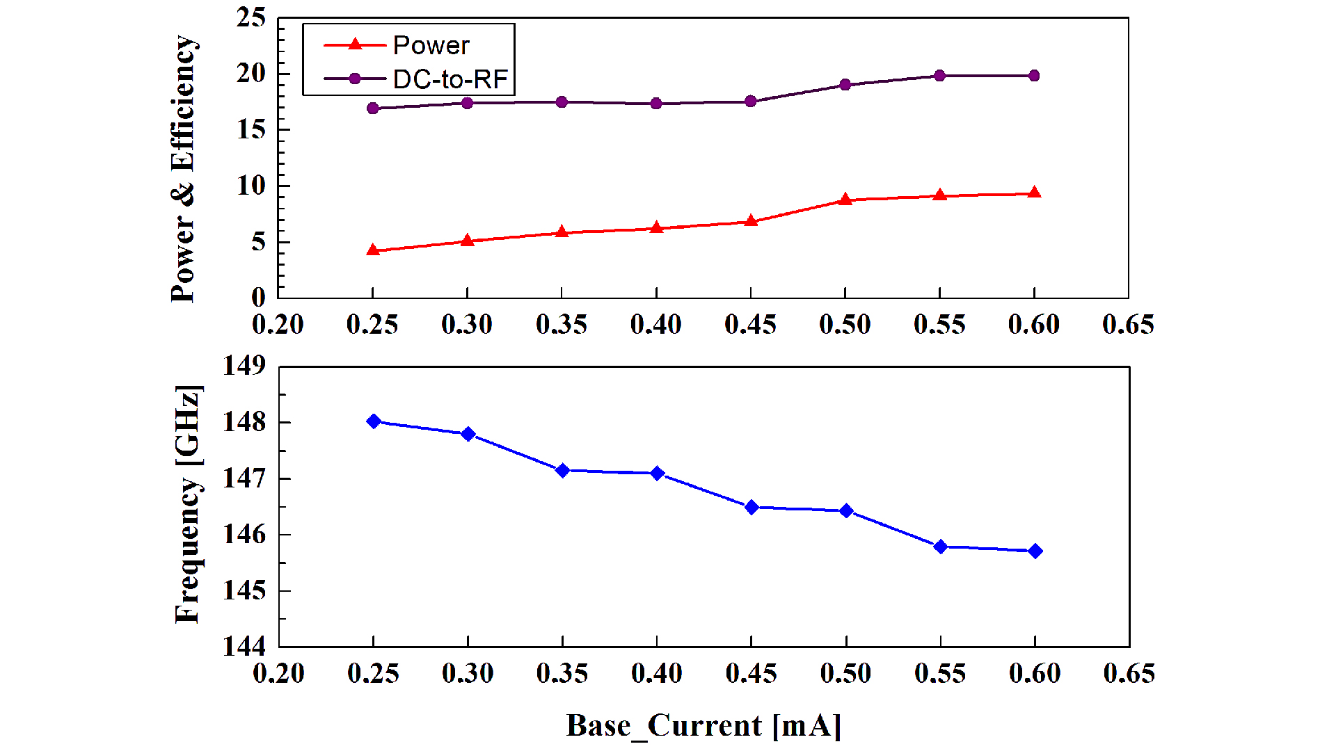
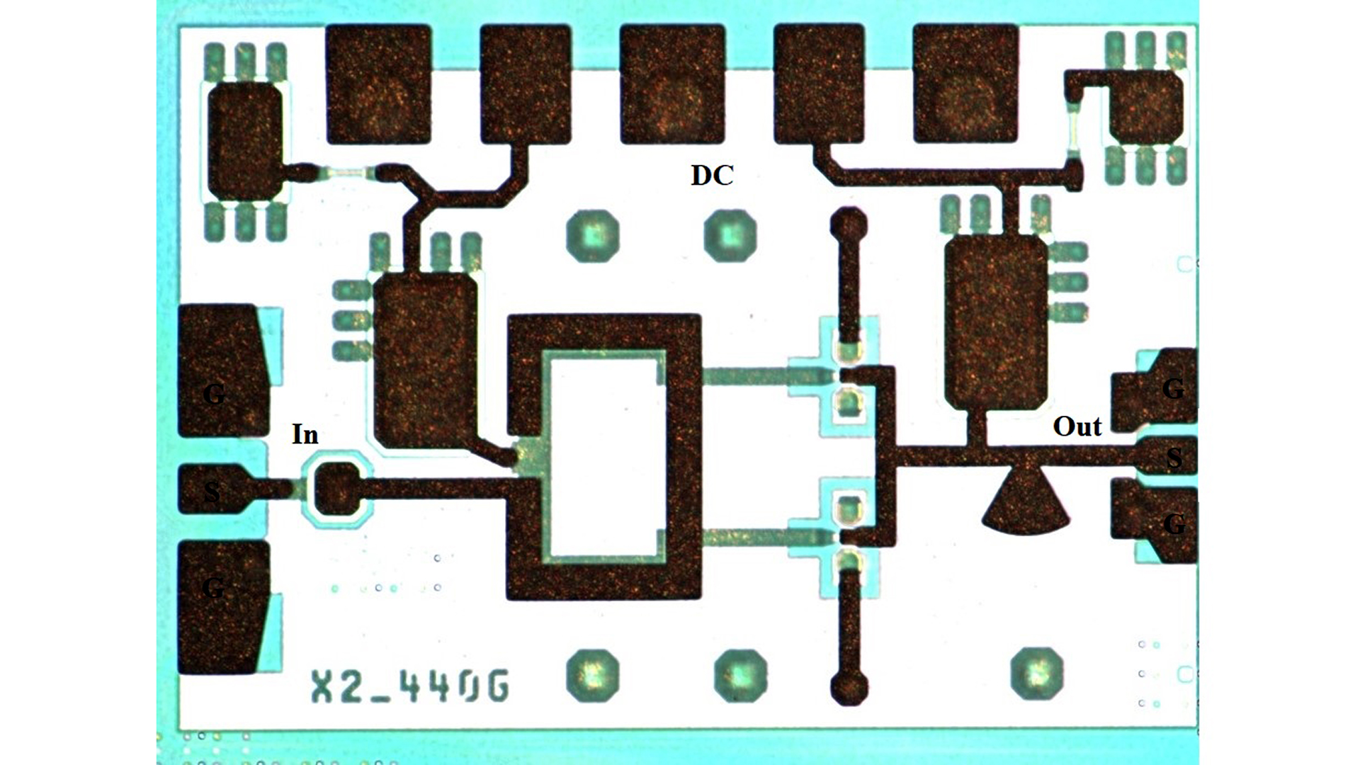
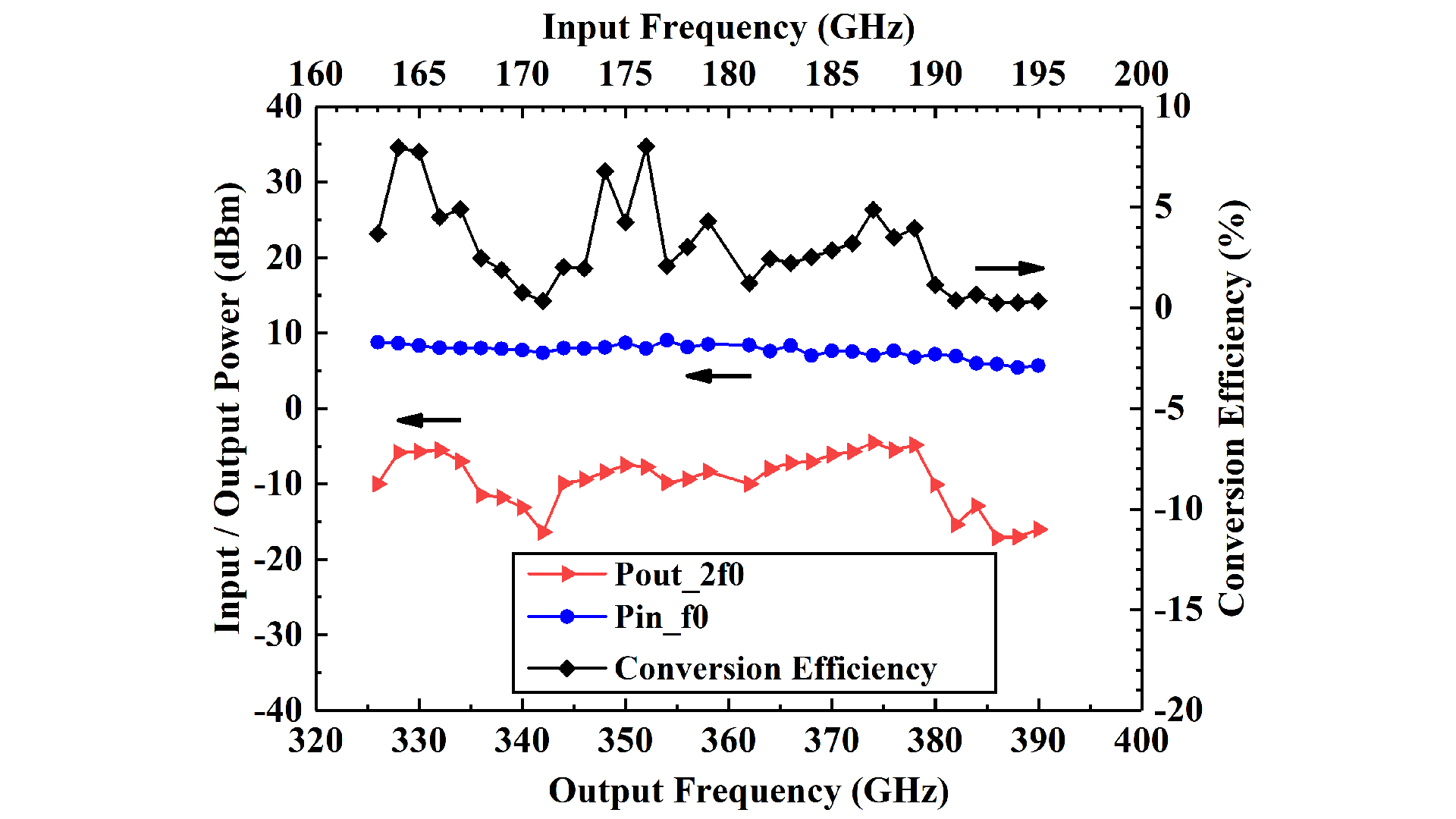
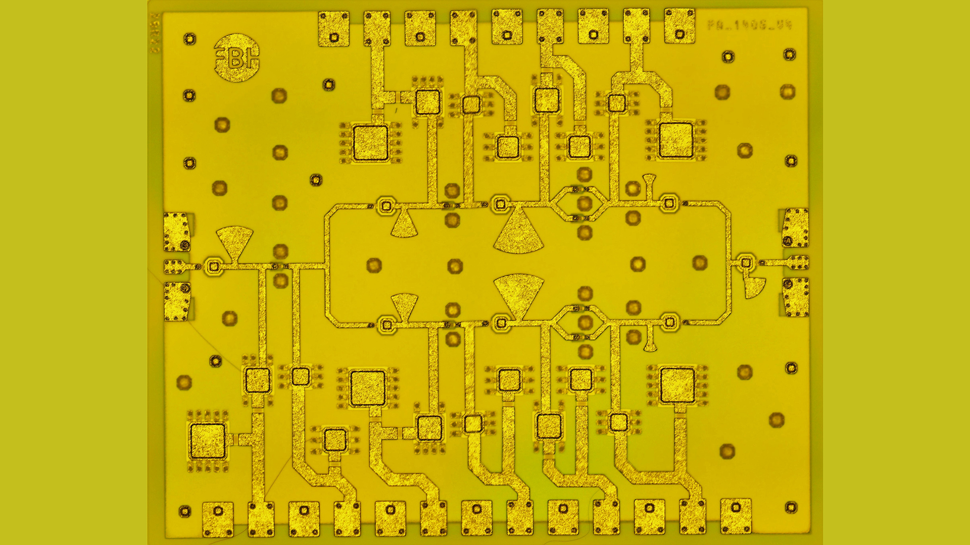
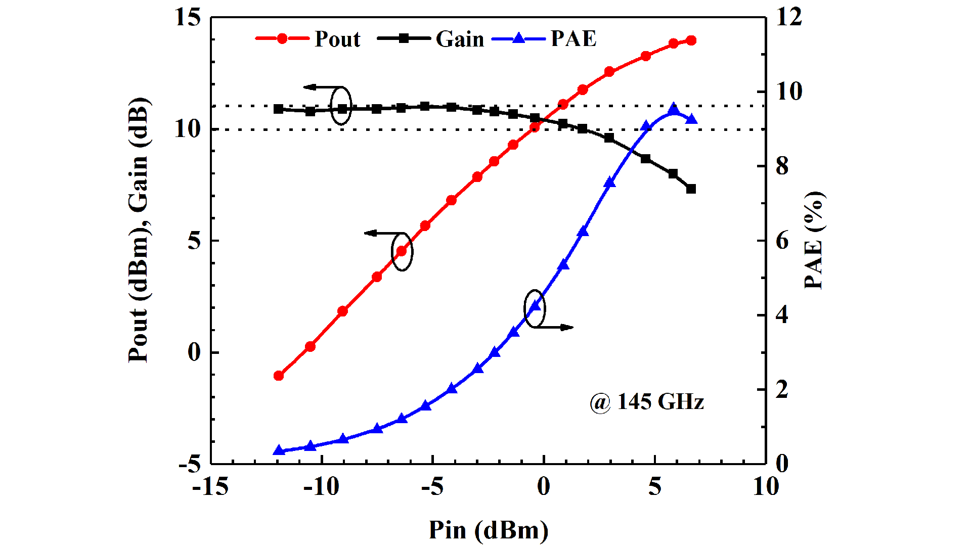
Realized InP-DHBT MMIC circuits for communication and radar applications at frequencies > 100 GHz