Materials Technology
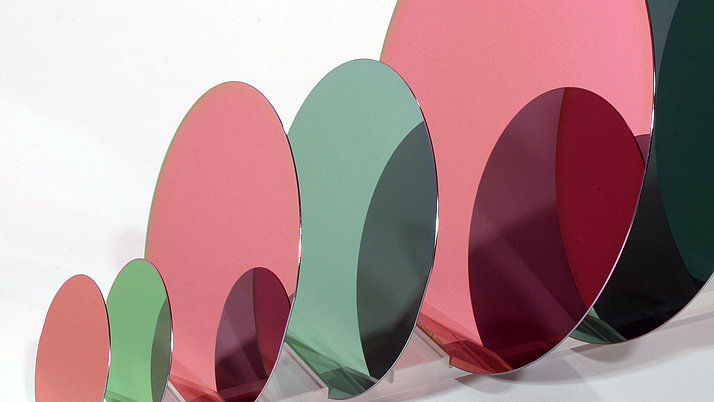
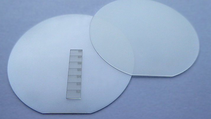
As a competence center for metalorganic vapor phase epitaxy (MOVPE), we produce ultrathin semiconductor layer structures with precisely defined crystalline properties. We use the material systems (Al,Ga)As, (Al,Ga,In)P, (Ga,In)(As,P) und (Al,Ga,In)N and suitable dopants to realize conductivities, refractive index and band gap profiles as well as absorption and emission characteristics in the UV, visible, and near-infrared wavelength range. These wafers can then be further processed into electronic or optoelectronic devices.
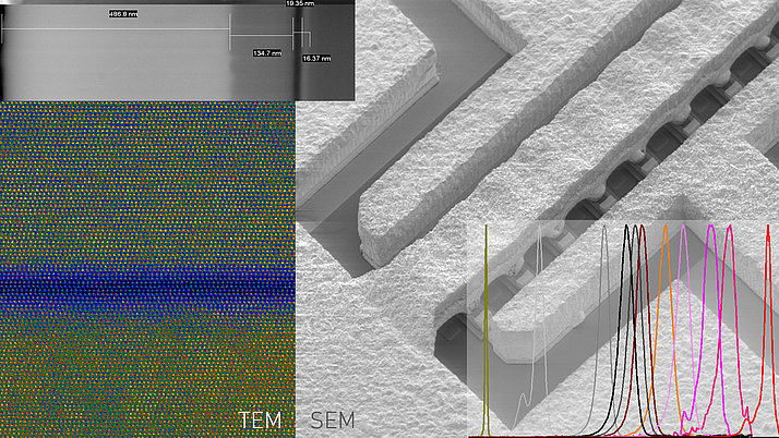
We monitor the development and optimization of devices using a variety of analytical methods, focusing on optical, electrical, and structural characteristics. The analytical methods are also used to analyse degradation and failure causes of devices.


![[Translate to English:] Flyer "III-V Technology"](/fileadmin/_processed_/0/5/csm_III-V_Technology_16f05911c0.png)
![Technology Offer FBH [Translate to English:] Flyer "Technologieangebot FBH"](/fileadmin/_processed_/7/2/csm_Technologieangebot_FBH_2024_c7eca08a96.png)
![[Translate to English:] Flyer "Frequent Nr. 13 (2020)"](/fileadmin/_processed_/4/6/csm_frequent_13-2020_online_15085b7a72.png)