Qualification of Epitaxial Layers
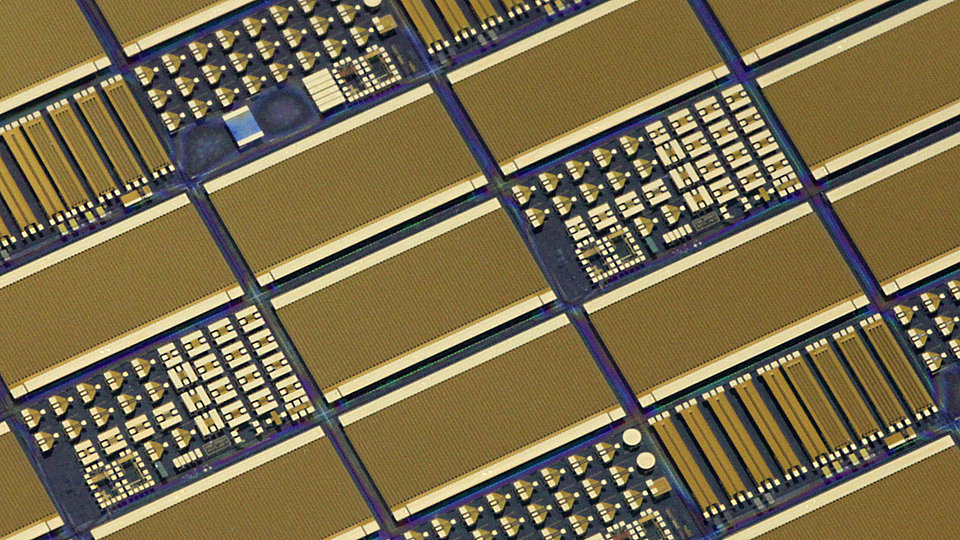
We qualify epitaxial layers using a stable device process. It is well known that non-destructive material investigations as usually applied for epixial wafer characterization may not be able to assess whether the layers are really suitable for device applications. The electrical behavior of a completely processed device is therefore considered a very reliable indicator for the quality of device epitaxy.

We offer epi-layer qualification processes for the following device technologies:
- transistors towards GaN MMICs in 0.25 µm technology
- lateral GaN power transistors in p-GaN and Schottky-gate technology