UV Light Emitting Diodes (UV-LEDs)
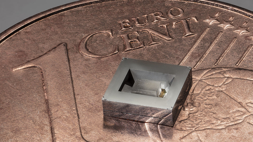
We develop (In)AlGaN-based light-emitting diodes (LEDs) with emission in the ultraviolet (UV) spectral region. The research work takes place in close cooperation with the TU Berlin within the Joint Lab GaN Optoelectronics. Activities include device simulation, design, epitaxy of (InAlGa)N heterostructures, device chip fabrication, assembly and characterization.
Advantages of our UV-LEDs at a glance
- emission wavelength can be adjusted to the respective application by adapting the heterostructure
- small, compact and robust
- can be operated at low voltages (mobile applications)
- can be switched quickly
- do not contain toxic substances
Thanks to these properties, UV LEDs are already superior to conventional UV emitters such as mercury-based gas discharge lamps in many respects. As technology advances, the advantages of UV LEDs will continue to increase.
Current research focus:
- 300-320 nm for surface polymerization, phototherapy and plant irradiation, typ. light output power 25 mW (350 mA)
- 230-235 nm for skin tolerant UV antiseptics, typ. light output power 6 mW (200 mA)
- 225-230 nm for gas sensing, typ. light output power 0.25 mW (200 mA)
Previous wavelength ranges:
- 260-280 nm for water, air and surface disinfection, typ. light output power 18 mW (350 mA)
- 250-260 nm for spectroscopy, typ. light output power 9 mW (350 mA)
Our best UV LEDs achieve up to twice the light output power as specified above. Together with our in-house Prototype Engineering Lab, we assemble our UV LEDs into lamp modules and complete irradiation systems. We test these with partners in practical applications such as plant irradiation or wound and skin disinfection.
- simulation of the LED heterostructure
- epitaxial deposition of the (InAlGa)N heterostructures on different MOVPE machines
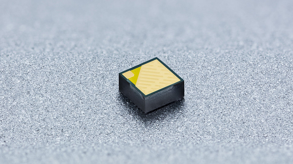
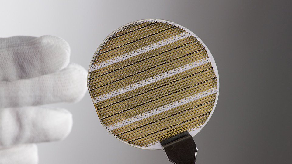
- chip technology in the process line of the FBH clean room (including monolithically integrated gold micro-stud-bumps for subsequent flip-chip assembly via thermocompression)
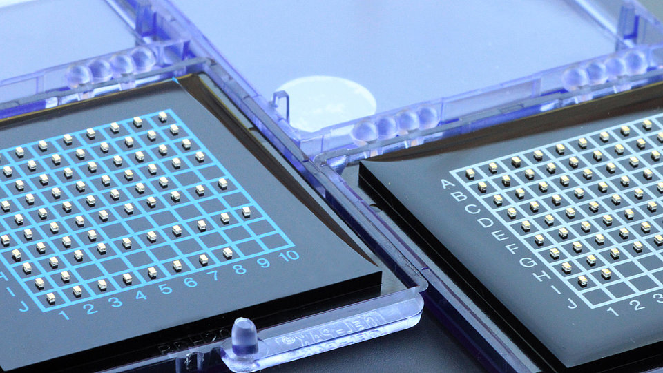
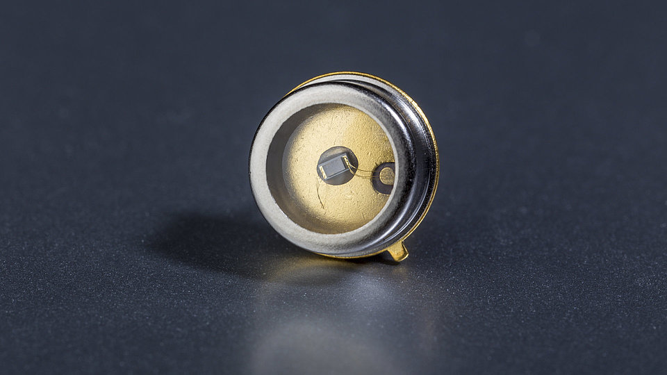
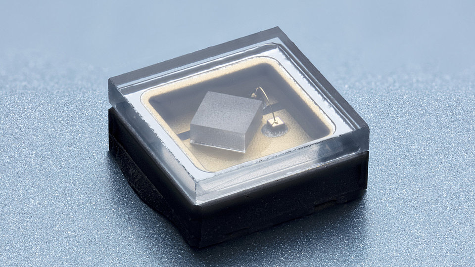
- assembly of LED chips in SMD packages made of AlN ceramics or crystalline silicon, which can be sealed with lens covers
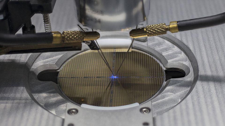
- characterization (including measurement of the power-current-voltage characteristics as well as their spectra on-wafer or on the mounted chip, detailed aging studies to analyse possible degradation mechanisms)