A new method of monolithic GaN HEMT integration using mechanical strain tuning
Fig. 1: Electronic properties in the 2DEG region with (reduces 2DEG electron density) and without (increases 2DEG density) applied external compressive strain
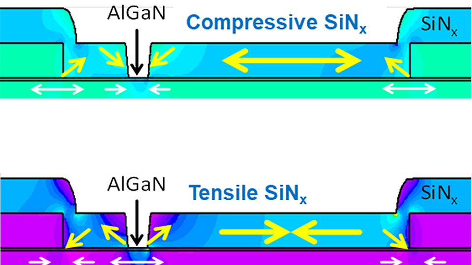
Fig. 2: Simulation of mechanical stress properties in the vicinity of a gate trench structure for a compressive and a tensile SiNx passivation layer
The channel electron density in GaN field effect transistors (2DEG) depends on the difference between spontaneous and piezoelectric polarization vectors in the respective layers forming the heterointerface. This results in a 2DEG formation whose density solely depends on the different degrees of built-in polarization in the respective materials. In GaN HEMTs with AlGaN/GaN heterojunctions, the Al concentration of the barrier layer is usually selected such that an optimum 2DEG electron concentration for a specific application can be achieved. For a given gate technology, this pre-setting results in a characteristic pinch-off voltage of the devices.
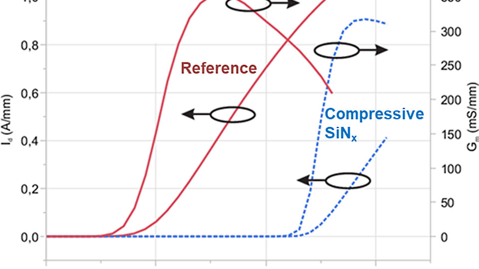
As shown in Fig. 1, any variation of the piezoelectric polarization in the AlGaN can also alter 2DEG electron concentration. It immediately changes if the AlGaN layer is mechanically compressed or extended. For instance, this can be achieved locally by applying tensile or compressively stressed passivation layers in conjunction with trench etching through the same layer. The built-in mechanical stress at the trench sidewalls in the layer relaxes and therefore applies mechanical strain to the semiconductor material underneath the corners and in the trench gap. Two-dimensional mechanical simulations, as shown in Fig. 2, compare the effect of tensile and compressively stressed SiNx passivation layers on the mechanical properties in vicinity of a 150 nm sub-µm trench. This represents a typical device geometry which is, for example, used in FBH's Ka-band MMIC process. Tensile stressed passivation introduces a tensile strain in the trench, whereas a compressively stressed passivation layers results in a compressive strain. According to Fig. 1, tensile mechanical strain leads to electron accumulation, whereas compressive strain leads to depletion. As trench etching is the first step in a trench gate fabrication process it is now possible to intentionally modify the 2DEG concentration immediately underneath the gate and thus to engineer the threshold voltage levels of respective transistors. The simulation also shows that the mechanical strain introduced at the trench corners has its maximum value there and decays towards the center of the trench. Thus, the effectivity of mechanical strain introduction increases with decreasing trench dimensions. For very short gates trenches (< 150 nm) practically the whole gate region is affected resulting in pronounced threshold voltage shift. Fig. 3 compares the DC properties of 150 nm devices fabricated by using passivation layers with different built-in stress levels. It shows that when introducing a compressive SiNx passivation layer with a stress of 900 MPa it is even possible to fully deplete electrons underneath and therefore render devices normally-off.
This new technique is extremely versatile. It is now possible for the first time to intentionally utilize processing parameters to tailor device properties for certain applications without changing design of the epitaxial layer sequence. This enables monolithic integration of different device functionalities on one chip.
This work was supported by the European Community through the FP7 project “GaNSaT” under EC—Contract 606981.
Publication
K. Osipov, I. Ostermay, M. Bodduluri, F. Brunner, G. Tränkle, and J. Würfl, "Local 2DEG Density Control in Heterostructures of Piezoelectric Materials and Its Application in GaN HEMT Fabrication Technology", IEEE Trans. Electron Devices, vol. 65, no. 8, pp. 3176-3184 (2018).


