Chalmers GaN HEMT Charge Model – Revisited
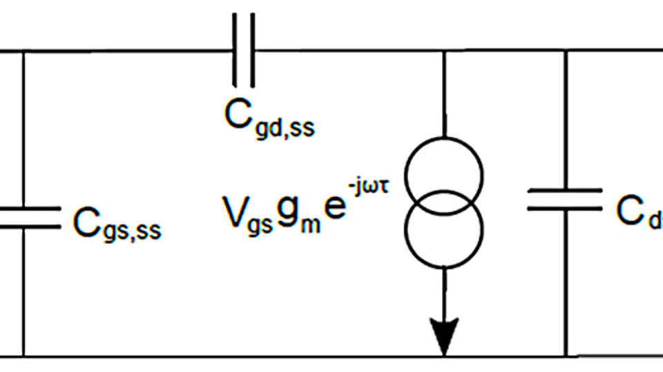
Fig. 1: Intrinsic small-signal equivalent circuit in π-configuration. For simplicity, the intrinsic resistances are neglected.
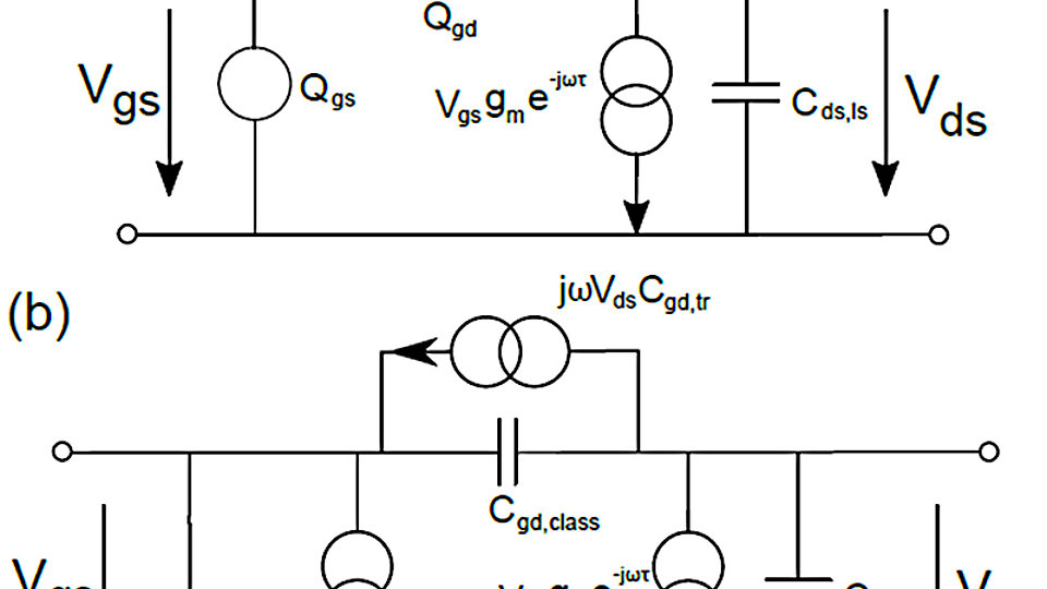
Fig. 2: (a) Large-signal equivalent circuit of the intrinsic GaN HEMT. (b) Intrinsic large-signal model in the presence of transcapacitances Cgs,tr and Cgd,tr parallel to Cgs,class and Cgd,class
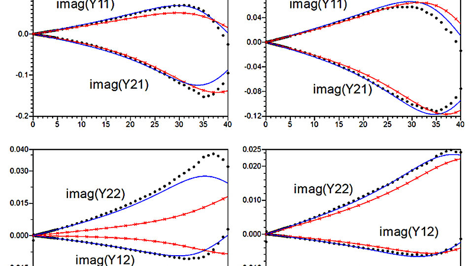
Fig. 3: Measured and simulated values of imaginary part of Y-parameters up to 40 GHz at Vgs = -2 V and Vds = 16 V, and 28 V, (black: measurements, red: using capacitance model parameters for charge model, blue: parameters extracted accounting for transcapacitance effects)
In the microwave domain, the transistor behavior is determined to a significant extent by the charges stored in the device. This can be observed in form of capacitances and transit times. When deriving a large-signal model for circuit design, one faces the difficulty that bias-dependent capacitances and transit-times are determined from measurements that represent only time-derivatives of the real physical quantity, the stored charges.
The Chalmers model is one of the frequently used and well-known GaN HEMT models, featuring two implementations of the capacitive effects. It offers both a solution allowing to simply describe the bias-dependence of the capacitances (capacitance model) and a charge-based model. Both models share the same set of parameters, but fitting the capacitance-model parameters to measurement-extracted values would not yield an equally good description when switching to the charge-based model. On the other hand, staying with the capacitance-based model is depreciated as it intrinsically contradicts the device physics. It is also known to lead to non-convergence problems in simulations.
It was therefore required to analyze the differences between the two implementations concerning the meaning of the model parameters. The small-signal model topology of an intrinsic GaN HEMT is shown in Fig. 1. It basically consists of gate-source, gate-drain, and drain-source capacitances and the transconductance. The respective large-signal model is shown in Fig. 2a. The bias-dependent gate-drain and gate-source capacitances are represented by charges Qgs(Vgs,Vds) and Qgd(Vgd,Vds). The discrepancy between the two representations becomes obvious when a small-signal representation is determined. It is mainly due to transcapacitances that result from calculating the time-derivative of the charges Qgs and Qgd, known to be functions of both gate and drain bias voltages. The corresponding small-signal equivalent circuit is shown in Fig. 2b. Theoretically, transcapacitances can be obtained by partial derivation of the charge to the voltage across a remote set of terminals (remote voltage), while classical capacitances are derived by partial derivation of the charge to the voltage across the capacitor’s terminals, which would directly result in capacitance functions in the capacitance model.
The intrinsic small-signal model in π-configuration as illustrated in Fig. 1 is used as basis for the large-signal model parameter extraction. Its parameter values are extracted from multi-bias S-parameter measurements after de-embedding the extrinsic elements extracted from cold-FET measurements. Fig. 2(b), in contrast, illustrates the small-signal topology derived from the charge-based large-signal model considering transcapacitances. Transcapacitances represent the current caused by the time-derivative of a remote voltage and are thus drawn as current sources multiplied with jω.
The difference in the circuit topology is obvious. In order to establish an approximate correspondence in the circuit behavior, the Y-parameters Y11 and Y21 for the circuit of Fig. 2b are rewritten in the following form:
Y11,ls = jωCgs,class + jω(Cgd,class – Cgd,tr) + jωCgd,tr
Y21,ls = gm,ls (1-jωτls) – jω(Cgd,class - Cgd,tr) – jωCgd,tr
This way, as long as we have a negligible Cgs,tr to Y12 and a negligible Cgd,tr to Y11 and Y21, the small-signal and large-signal capacitances can be easily related to each other.
Fig. 3 shows the values of imaginary part of Y-parameters calculated from measured S-parameters biased at Vg = -2 V and Vds = 16 V, and 28 V. They are compared to those simulated by using capacitance model parameters for the charge model (red marked lines) and using the extracted charge model accounting for transcapacitance effects (blue solid lines). A significantly improved modeling accuracy can be achieved at all bias conditions for Y12 and Y22 by using the extracted charge model when the transcapacitance Cgd,tr is taken into account. This testifies the importance of transcapacitances to intrinsic capacitance Cgd modeling as well as to charge modeling.
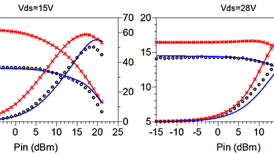
Fig. 4 shows the comparison between measured and simulated gain and PAE using capacitance model parameters for the charge model in contrast to using the extracted charge model accounting for transcapacitance effects as derived in this work. For the prediction results of gain and PAE, a significantly improved agreement can be observed at all bias conditions by using the extracted charge model if the transcapacitances are accounted for. This improvement can be attributed to the better prediction of the intrinsic capacitance Cgd and S-parameters. Moreover, the dramatic discrepancies found in the prediction of the linear gain at each bias by using the capacitance model parameters for the charge model also indicate the terrible modeling accuracy of the intrinsic capacitances when supplying the capacitance model parameters in the charge model.
References
P. Luo, F. Schnieder, and M. Rudolph, "Chalmers GaN HEMT charge model revisited", in 2018 11th German Microwave Conference (GeMiC), pp. 164–167, Mar. 2018.
L. Angelov, H. Zirath, and N. Rosman, "A new empirical nonlinear model for HEMT and MESFET devices", IEEE Transactions on Microwave Theory and Techniques, vol. 40, no. 12, pp. 2258–2266, Dec. 1992.
I. Angelov, L. Bengtsson, and M. Garcia, "Extensions of the Chalmers nonlinear HEMT and MESFET model", IEEE Transactions on Microwave Theory and Techniques, vol. 44, no. 10, pp. 1664–1674, Oct. 1996.


