Defect-sensitive etching to monitor reduction of dislocation densities in AlGaN
Fig. 1: Etch pits around dislocations in AlGaN layers with low and high aluminum concentration. Large etch pits form around screw-type dislocations, smaller pits around edge-type dislocations.
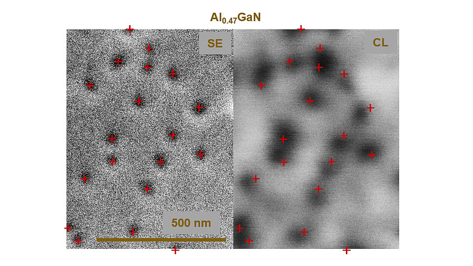
Fig. 2: Etch pit positions (SE image) and dark spot positions (CL image) correlate. Due to strain fields around dislocations, a locally varying band gap energy, and tilt of TD, the center of dark spots is typically slightly offset from the position where dislocations end at the surface of the layer.
At FBH, we develop UVC LEDs for disinfection and high-power transistors with high breakthrough voltage required for automotive electronics. Integral elements of these devices are semiconductor heterostructures based on AlGaN layers. These AlGaN layers are grown heteroepitaxially on substrates with differing lattice constants. As a consequence, high densities of dislocations are generated at the substrate-semiconductor interface. Many of them run in growth direction as threading dislocations (TD) through the AlGaN layers. These dislocations negatively impact the current flow in transistors and light generation efficiency in LEDs. Reducing the density of TDs (TDD) through crystal growth optimization is a key challenge to improve device performance. Therefore, methods are required to determine the TDD in a reliable and exact way.
We have tested and verified a defect-sensitive etching method with Ba(OH)2/MgO etch drops on surfaces of AlGaN layers across the whole composition range from GaN to AlN. The etchant selectively etches the AlGaN surface only around the dislocations, resulting in hexagonal-shaped etch pits. These can be counted in secondary electron images (SE) obtained by scanning electron microscopy or atomic force microscopy topograms. This approach enables access to both the density and spatial distribution of dislocations. Additionally, the etch pits become wider if the dislocations have larger Burgers vectors, allowing to differentiate between edge-type and screw-type dislocations.
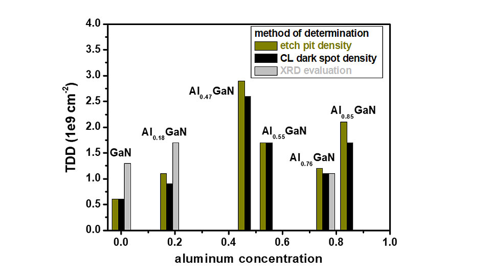
We verified that each dislocation forms an etch pit by comparing with previously used methods, such as counting cathodoluminescence (CL) dark spots around dislocations or evaluating XRD linewidths, which are broadened by dislocations. The etch pit method offers several advantages over the other methods. The spatial resolution in cathodoluminescence is limited to approximately 100 – 250 nm due to carrier diffusion determining the minimum diameter of dark spots. Etch pit counting provides a resolution ten times finer. Additionally, the etching method can also be used for AlGaN layers with aluminum concentrations > 90 %, where the AlGaN layers usually do not provide enough luminescence for CL measurements. In contrast, the XRD method is based on models assuming a homogeneous distribution of dislocations, and neglecting further broadening mechanisms on XRD curves. These assumptions are not always correct, causing deviations in the derived TDD of up to a factor of 2. Therefore, the defect-sensitive etching method provides exact and more reliable feedback for optimizing AlGaN growth processes.


