Fast and efficient switching with GaN-based power-transistors

Fig. 1: 100 mΩ / 300 V GaN switching transistor with 4.5 mm × 2.4 mm die size on a 3" wafer
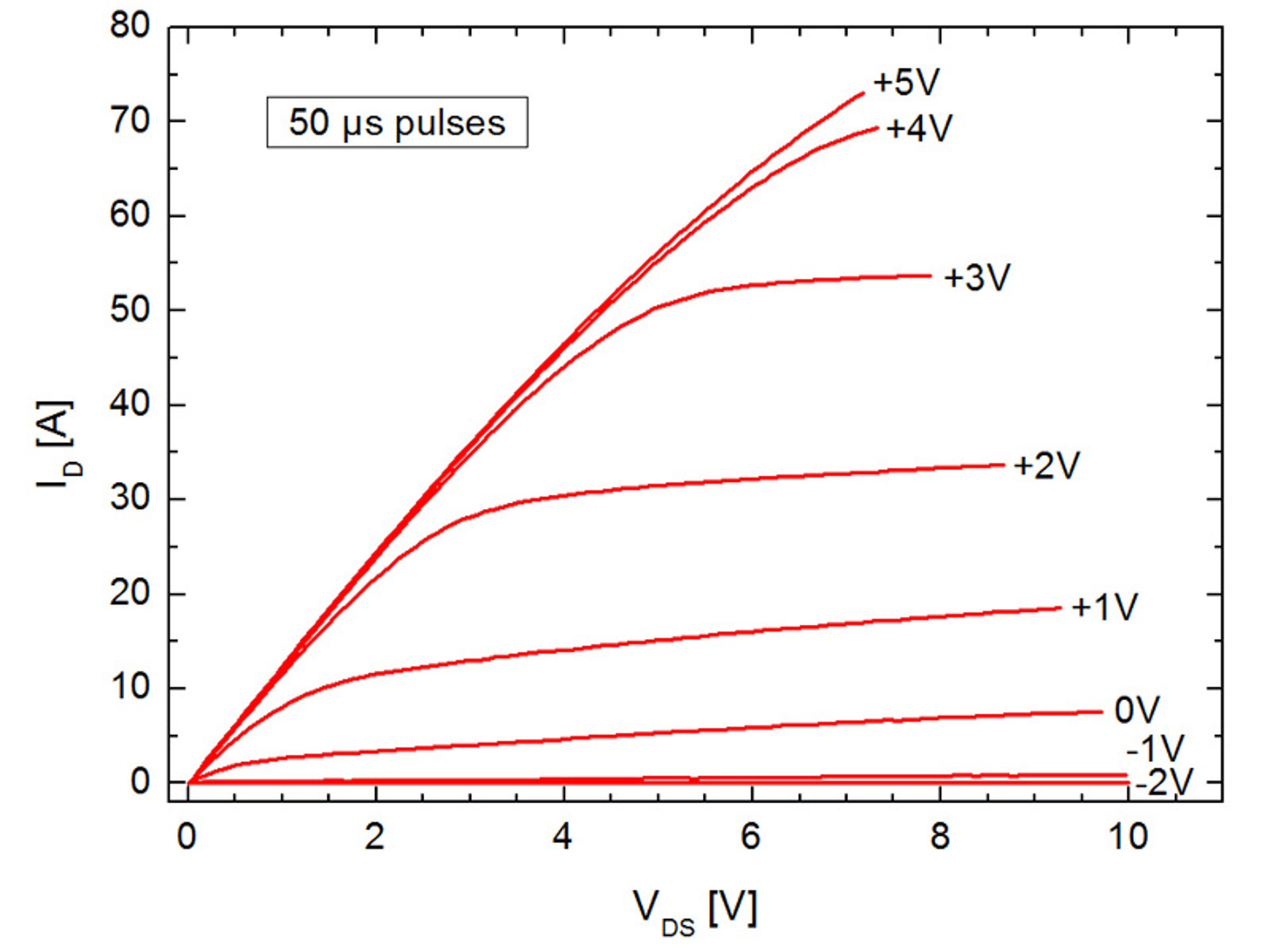
Fig. 2: Pulsed output characteristic of a GaN power transistor in p-GaN gate technoloy with 150 mm gate width showing an on-state resistance of RON RON = 80 mΩ for 5 V gate bias
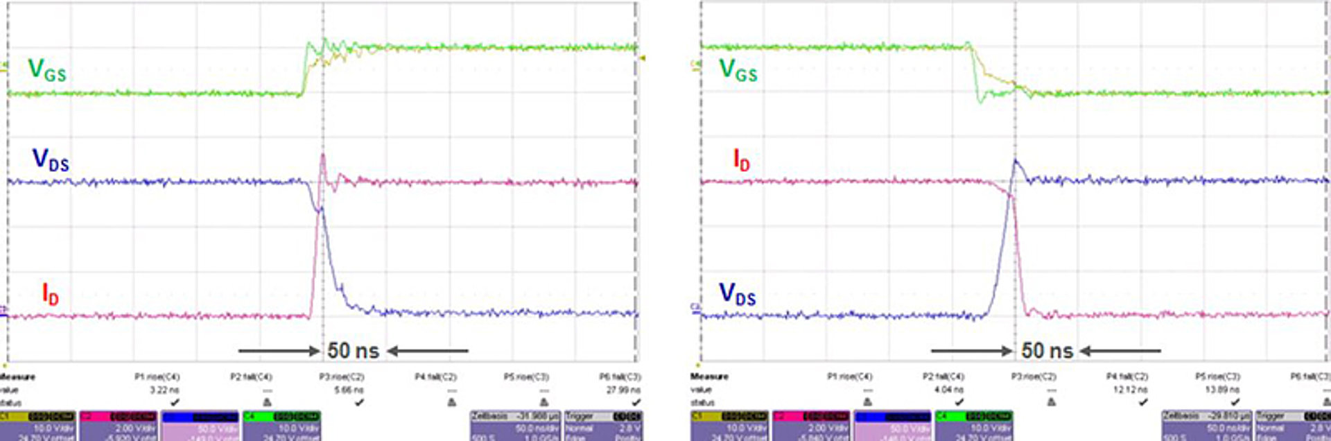
Fig. 3: Switching transients from off- to on-state (l) and from on- to off-state (r) for a GaN transistor with 150 mm gate width for 150 V blocking voltage and 6 A on-state current. The rise and fall times are 20 ns, respectively. Measurements: TU Berlin
Light weighted and small volume electronic power converters are desirable for automotive and other mobile applications. Technically, such features are achieveable by increasing the switching frequency, which enables smaller and more light weighted passive components such as, for example, inductors. However, a key requirement is the availability of efficient power switching transistors.
The transition time between transistor on-state (low conduction losses due to low voltage drop at high current) and transistor off-state (low losses due to low leakage current at high bias) should be as short as possible to minimize switching losses. Current flow and drain bias are simultaneously present in this period and thus generate thermal loss. The gate charge required to open or to close the transistor channel determines the switching speed. The product of on-state resistance RON and gate charge QG is thus a benchmark for switching losses inherent to a certain transistor technology.
GaN-based high-voltage switching transistors simultaneously show a low area-specific on-state resistance and a low gate capacitance. This enables particularly low switching losses and therefore efficient high-frequency converters.
The FBH develops normally-off GaN transistors based on a p-GaN gate technology. Switching transistors with 150 mm gate width have been realized showing an on-state resistance RON = 100 mΩ and a maximum pulse current of 75 A for 300 V blocking strength.
A double-pulse switching set-up with inductive load and a time resolution < 5 ns has been realized at the TU Berlin, Power Electronics Department to analyze the switching properties of the FBH transistors. The rise and fall time of the switching events were both determined to 20 ns only when the transistors were switched between an off-state voltage of 150 V and a current load of 6 A. For 1 MHz switching transistor losses would thus be present only for < 10% of the total cycle. The gate charge required for the transistor switching event was determined as QG = 5.5 nC. The resulting product RON x QG should be as small as possible. For the tested GaN transistors optimized for 300 V blocking voltage RON x QG is only 0.55 ΩnC and therefore 4 times better than compared to competitive Si devices featuring the same blocking voltage.
Publications
O. Hilt, F. Brunner, E. Cho, A. Knauer, E. Bahat-Treidel, J. Würfl, "Normally-off High-Voltage p-GaN Gate GaN HFET with Carbon-Doped Buffer", Proc. Int. Symp. on Power Semiconductor Devices & IC's (ISPSD), San Diego, CA, May 23-26, pp. 239-242 (2011).
O. Hilt, E. Bahat-Treidel, E. Cho, S. Singwald, J. Würfl, "Impact of Buffer Composition on the Dynamic On-State Resistance of High-Voltage AlGaN/GaN HFETs", Proc. Int. Symp. on Power Semiconductor Devices & IC's (ISPSD), Bruges / Belgium, 3-7 June, pp. 345-348 (2012).
N. Badawi, P. Knieling, S. Dieckerhoff: "High Speed Gate Driver Design for Testing and Characterizing WBG Power Transistors", Proc. EPE-PEMC (2012).
FBH research: 20.11.2012