Flip-chip – a promising mounting technology for THz applications
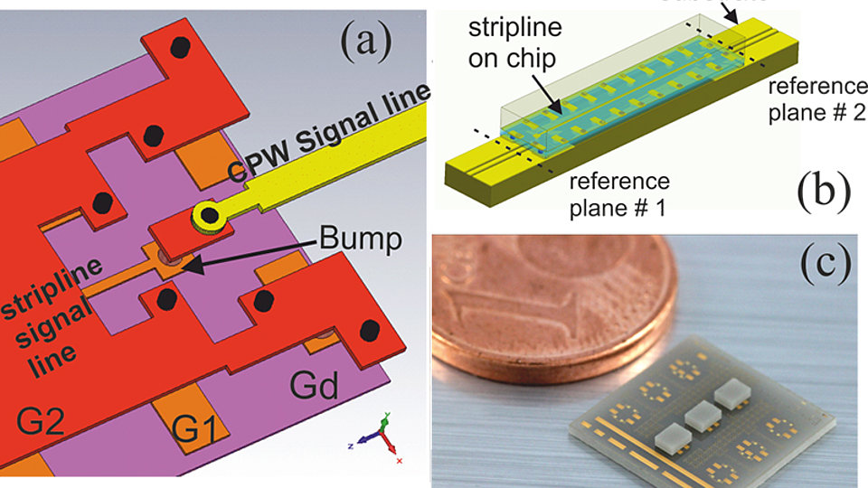
Fig. 1: (a) 3D view of flip-chip transition, (b) back-to-back flip-chip test structure, (c) fabricated module with 3 chips bonded on AlN substrate
Flip-chip connections offer shorter interconnection paths as compared to wire bonding, thus enabling higher bandwidth. The use of front-end semiconductor fabrication techniques allows for the accurate definition of thin-film waveguide structures leading up to the flip-chip connection, resulting in predictable EM behavior up to 500 GHz.
Recently, FBH has successfully developed flip-chip mounts operating up to 250 GHz, including a stripline-to-coplanar waveguide RF transition. The on-chip RF connections were realized as gold (Au) / benzocyclobutene (BCB) stripline waveguides, with an approximately 10 µm wide Au signal line sandwiched between top and bottom Au ground planes. BCB was used as a low-k interlayer dielectric.
The aluminum nitride (AlN) submount featured gold-plated coplanar waveguides (CPWs); interconnecting structures were realized with 10 µm diameter AuSn microbumps consisting of a multilayer metal stack with eutectic Au80Sn20 composition. Finally, the chips were placed onto the submount with the help of a semiautomatic flip-chip aligner with ±1 µm lateral alignment accuracy, within the design margin of ±2 µm. In the flip-chip bonding process, the chips and the substrate are briefly heated to above 300°C, leading to the alloying of the Au/Sn microbumps into the substrate’s Au contacts. Hence an electrical and mechanical connection between the chip and the substrate is formed.
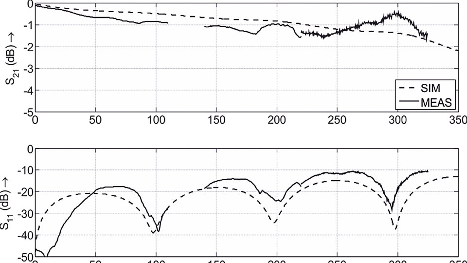
Small-signal RF measurements of back-to-back flip-chip transitions showed an insertion loss below 1.0 dB per interconnect, and a return loss of more than 10 dB from DC up to 250 GHz. These figures are so far the best reported flip-chip mounts in this frequency range.
FBH research: 17.11.2014

