GaN digital outphasing power amplifier – targeting efficient 5G communications
The next-generation wireless communication infrastructure demands for high flexibility, low cost and high efficiency. This goes along with the growing need for wideband, multi-band, and multi-standard features. In this context the all-digital transmitter chain represents the smartest solution. The analog output signal is encoded in a binary pulse sequence, so that the only analog component left is a bandpass filter at the power amplifier (PA) output just before the antenna. As a consequence, the PA becomes a pure switch. Future wireless communication standards will be based on very broadband signals with high peak-to-average power ratios (PAPR) in the 10 – 12 dB range. These characteristics, however, are responsible for one of the most crucial problems of digital PAs up to now, the significant degradation of efficiency at high power back-off (PBO) values. The values achieved so far are not fully competitive to analog concepts like Doherty or envelope tracking. One promising solution to overcome these limits is the digital outphasing concept.
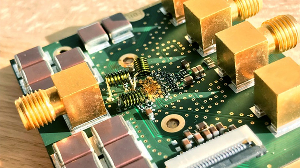
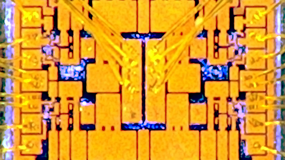
In October 2019, FBH has presented a digital GaN-based outphasing PA module (Fig. 1) for the microwave range at the European Microwave Conference (EuMC) 2019 in Paris (France). This module includes two GaN amplifier MMICs (Fig. 2) and hybrid input/output circuitry for biasing, combining and filtering. The realized PA applies different degrees of resonant commutation (partly or full) with a novel output combiner for the voltage on the center output nodes, which is optimized for high efficiency in the power back-off region. Moreover, the amplifier uses novel high-side drivers for the push-pull final-stages to ensure efficient driving.
At the maximum output power of 5.8 W, overall efficiency reaches 59% and decreases down to 25% at 10 dB PBO. The simulated final-stage drain efficiency peaks at 71% (0 dB PBO), drops down to 62% at 7 dB, and reaches 67% at 10 dB PBO. Additionally, the final stage efficiency stays above 50% even down to 15 dB PBO. The total efficiency shows the potential of the proposed GaN-based digital outphasing approach.
This work was supported by the German Federal Ministry of Education and Research (BMBF) within the "Research Fab Microelectronics Germany (FMD)" framework under ref. 16FMD02.
Publication
T. Hoffmann, A. Wentzel, F. Hühn, W. Heinrich, "GaN Digital Outphasing PA", Proceedings of the 49th European Microwave Conference (EuMC) 2019, pp. 551 - 554, Paris, France.

