Highly Efficient High-Power G-band Frequency Multiplier in Transferred-Substrate InP DHBT Technology
The frequency range between 100 GHz and 1 THz offers large bandwidth for high-speed communications as well as improved spatial resolution for radar sensors and imaging systems due to the short wavelength. For all these applications, the frequency source is a key component. Needed are high output power within a broad frequency range and low dc power consumption. Fundamental frequency signal sources are difficult in this frequency range, as they require high device cut-off frequencies. Frequency multiplication offers an attractive alternative, allowing for lower cut-off frequencies and simplifying THz frequency generation since commercially available high output power signal sources can be used at the input of the multipliers.
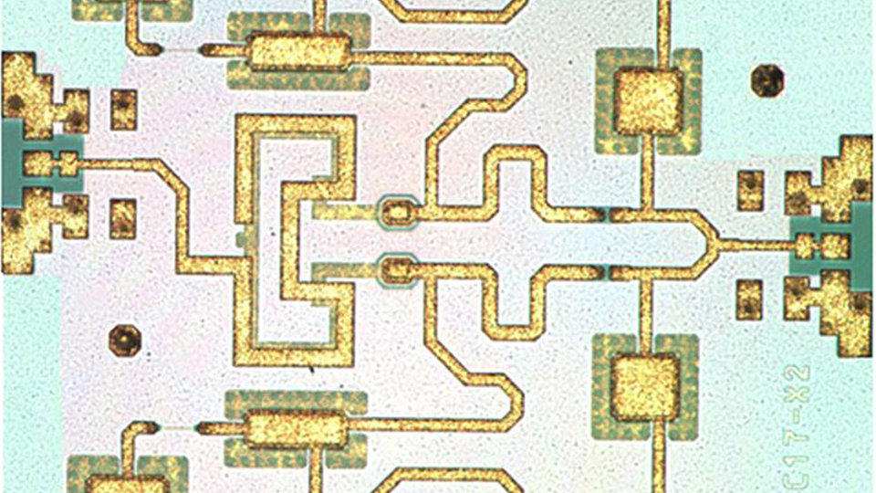
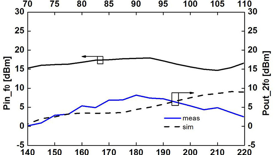
Recently, the FBH has published a full G-band (140-220 GHz) balanced frequency doubler with high output power in the IEEE Microwave and Wireless Components Letters. The MMIC technology is based on the 800 nm InP Transferred-Substrate DHBT high-speed process, developed at FBH. The doubler is based on a balanced topology. It contains a Marchand balun at the input, followed by the frequency doubler. The doubler delivers 5 dBm ± 3 dBm output power across the full band. The doubler circuit exhibits a power efficiency of 16% in this frequency range. This is the highest reported output power of an active frequency doubler with wideband frequency range. The figure shows a microphotograph of the doubler chip and the measured input and output power as a function of frequency.
Publication
M. Hossain, et al, “A Full G-band High Power Frequency Doubler in Transferred- Substrate InP HBT Technology,” IEEE Microwave and Wireless Components Letters, vol. 26, no. 1, pp. 49–51, January 2016.

