Improved heat dissipation for InP transistors – basis for more efficient and novel RF power circuits
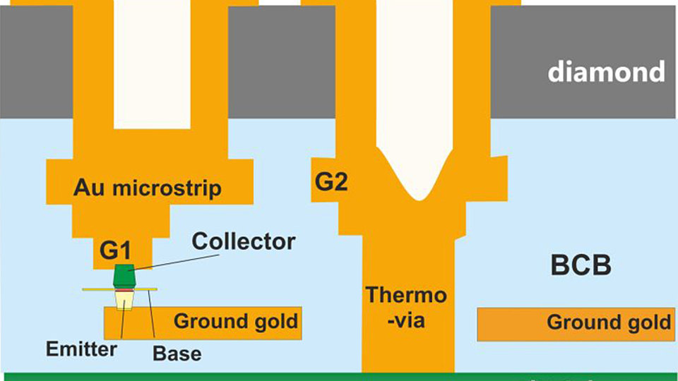
Fig. 1: Schematic cross section of the diamond layer integration into the InP DHBT transferred-substrate process (RF ground, G1, G2 and G3 – electroplated metallization layers)
Fig. 2: Thermal resistance versus dissipated heat. Data: extracted from IV curves taken on 1- finger HBT with 0.8×5 µm2 emitter size at different probe chuck temperatures (30°C - 50°C). Lines: averaged values of 1.1 and 4.2 K/mW with/without diamond heat sink layer
High RF output power and high efficiency are the keys to realize cost-effective subsystems in the mm-wave region between 100 and 300 GHz, enabling widespread adoption of many possible applications. These include, for example, security scanners, spectroscopy, high resolution radar, and medical and dental imaging. Indium Phosphide (InP) Double Heterojunction Bipolar Transistors (DHBTs) possess the key advantages of high breakdown voltage and high electron velocity, the combination of which enables to realize analog RF power ICs at 100 – 300 GHz and beyond. However, an important limit of the InP DHBT’s device operation lies in the thermal resistance Rth. The dissipated heat needs to be effectively removed from the transistor to keep the junction temperature inside the InP HBT lower than 125°C for reliable operation. Furthermore, RF gain and transistor efficiency are reduced with increasing junction temperature.
In the frame of the BMBF research project “Aufbau- und Verbindungstechnik für die Terahertz-Elektronik (AVTE)” (reference No.16V0060) improved heat dissipation from the InP DHBT active area and periphery was developed at FBH [1]. A thin-film diamond layer acting as heat spreader was added to FBH’s transferred substrate InP DHBT process. The resulting full MMIC integration includes three layers of interconnect metal, a thick gold ground plane, InP DHBTs, and passive capacitors and resistors embedded in BCB. Ceramic AlN is chosen as a host wafer for the InP substrate transfer because of its high thermal conductivity (170 W∙m-1∙K-1) and low microwave losses (see Fig. 1).
Diamond exhibits a very high thermal conductivity. We measured the thermal conductivity of the 10 µm thick nanocrystalline diamond layer to be within 600 and 800 W m-1 K-1, compared, for example, to silicon featuring 130 W m-1 K-1. With FBH’s diamond integration process, it was possible to lower the InP DHBT’s Rth to about 1 K/mW, compared to 4 K/mW for a baseline InP DHBT without thermal management (see Fig. 2). Besides, the diamond films exhibit a very low loss tangent up to THz frequencies, which make them a perfect dielectric for the high-power mm-wave application.
In principle, this advance would allow us to more than triple the power density of the InP DHBT device while maintaining the same junction temperature. Higher output power of a single transistor device is a significant enabler of efficient high RF power circuits. Although the circuit output power can be increased by putting many transistors in parallel, the RF power combining schemes are usually not very broadband and introduce passive losses.
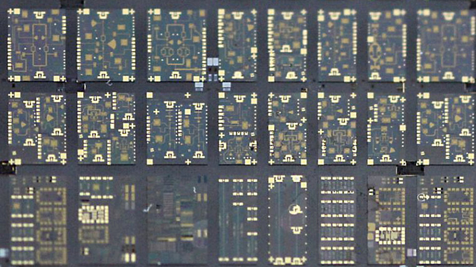
The key of FBH’s diamond integration is that the “hot” collector end of the InP DHBT can be heat sunk without connecting this lead to the RF ground. S-parameters in the frequency range up to 110 GHz were measured to determine the current gain cut-off frequency (ft) and the maximum oscillation frequency (fmax) for 1-finger HBTs with 0.8×5 µm2 emitter area. As expected, the RF performance shows only a slight degradation due to the thermal via connection of the collector to the diamond layer on top of the transistor. At IC = 20 mA and VCE = 1.5 V the average fT decreased from 358 GHz to 321 GHz after diamond integration, and the average fmax dropped from 329 GHz to 321 GHz only after diamond layer bonding. The DC curves exhibited higher device stability. The maximum collector current increased with diamond integration from 20 to 25 mA for a single-finger device. A detailed picture of a fully processed Diamond-InP DHBT wafer is shown in Fig. 4.
The diamond-integrated InP DHBT technology presented here is compatible with flip-chip mounting technology developed within the same research program [2]. To realize it, wafers were diced allowing subsequent flip-chip mounting and further characterization of the circuitry. In the project presented here, FBH’s goal is not only to research the basic device technology, but also to enable circuit and subsystem applications which are so far not accessible with existing technologies.
Publications
[1] K. Nosaeva, N. Weimann, M. Rudolph, W. John, O. Krueger, W. Heinrich, “Improved thermal management of InP transistors in transferred-substrate technology with a diamond heat-spreading layer”, Electronics Letters, Vol. 51, No. 13, S. 1010–1012; DOI: 10.1049/el.2015.1135 IET Digital Library
[2] S. Monayakul, S. Sinha, C.-T. Wang, N. Weimann, F. J. Schmückle, M. Hrobak, V. Krozer, W. John, L. Weixelbaum, P. Wolter, O. Krüger, W. Heinrich, "Flip-chip interconnects for 250 GHz modules", IEEE Microwave and Wireless Components Letters, Vol. 25, No. 6, S. 358–360, Juni 2015.


