Improved performance of UV-LEDs emitting around 300 nm
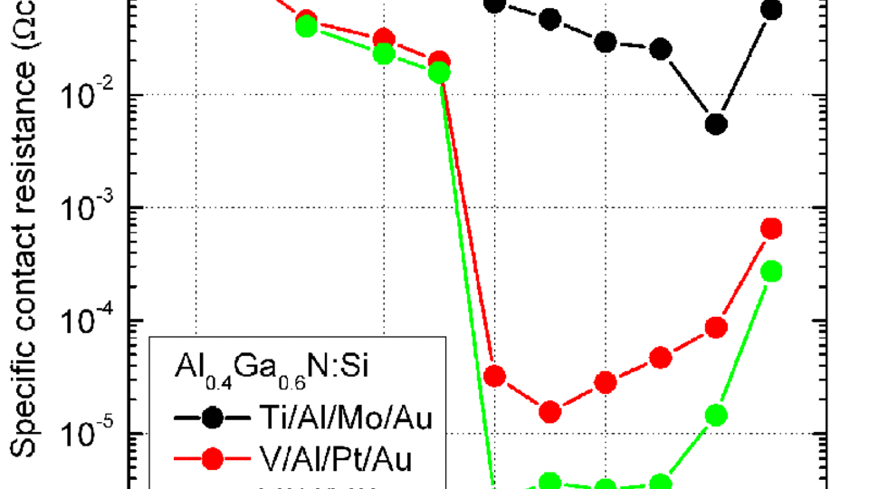
Fig. 1: Specific contact resistance of various contact systems on n-Al0.4Ga0.6N:Si in dependence on the annealing temperature.
Drying and curing of paints and coatings are considered as the dominant fields of application for UV LEDs for the next years. Currently, for this purpose mainly low-pressure mercury vapor lamps are used. If those lamps were replaced by UV LEDs with sufficiently high power and efficiency, the high voltage required to operate the light sources could be avoided. Moreover, the heavy metal mercury would not be needed anymore.
In our work we currently focus on LEDs with an emission wavelength in the UV-B range (280-315 nm) whose active region consists of an InAlGaN/AlGaN multi-quantum film structure. Based on our previous optimization of the layer design and the epitaxial growth conditions, which resulted in the reproducible demonstration of emission powers in the milliwatt range in on-wafer measurements with unprocessed wafers, we have now advanced the chip processing and mounting technology of our LEDs. Thus, we considerably improved the device performance. The redesign of the contacts was one of the major steps: Typically the n-side of an UV-B LED consists of Al0.4Ga0.6N:Si which forms an Schottky contact with conventional metal layer systems such as Ti/Al/Mo/Au and results in high operation voltages of the LED. By using Vanadium we succeeded in fabricating ohmic contacts with specific resistances in the 10-6 Wcm2 range. Fig. 1 shows that the novel contacts have resistances several orders of magnitude below our previous standard contacts Ti/Al/Mo/Au. With 700 °C the required annealing temperature is moderate and compatible with the remaining chip technology.
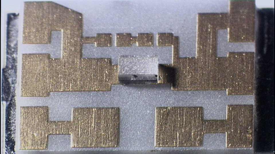
Another important step was to advance the chip mounting technology. To obtain a large output power from a single chip the heat has to be extracted efficiently from the active region. The previously used AlN submounts were only a few 100 µm larger than the chip itself which limited the lateral heat spreading. Fig. 2 shows a redesigned ceramic package whose larger area and additional thick copper core considerably reduces the thermal resistance. Moreover, the via contacts of the package allow for surface mounting.
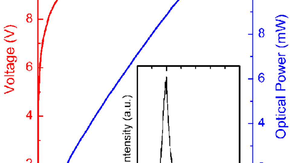
Characteristics and spectrum of an UV-B LED with optimized chip processing and mounting technology are shown in Fig. 3. The emission power thermally only rolls over at currents beyond 400 mA resulting in a light output power larger than 12 mW. The spectrum shows a dominant peak at a wavelength of 299 nm and only a weak emission in the UV-A range. Currently, we are studying the degradation of these LEDs under constant current operation and working on reducing the emission wavelength in the UV-C range.
FBH research: 03.01.2013


