MOVPE growth of polar (0001) and non-polar (11-20) GaN on cone-shaped patterned sapphire substrates
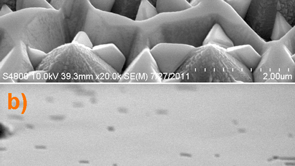
Fig. 1: Top view SEM pictures of (0001) GaN grown on CPSS after 20 min growth time (a), side view after 90 min (b).
The patterned sapphire substrates (PSS) technology based on lateral overgrowth has been proven effective in reducing threading dislocation density and releasing in-plane residual strain of GaN. However, the concurrent formation of facets in dependence on growth conditions and their impact on stress and morphology evolution has not been studied in detail up to now. Especially, using non-c-plane oriented substrates requires control of layer orientation in order to avoid formation of different phases affecting crystallinity and morphology.
Therefore, growth on PSS has been investigated by Mrs. Mei-Tan Wang from National Taiwan University during her stay at FBH within the "Research visits to Germany of NSC sponsored Ph.D. Degree Candidates (Sandwich Program)", bringing together her experience in PSS and the competence of FBH in in-situ analysis of growth processes.
Surface topology, strain and structural quality of GaN grown by metalorganic vapor phase epitaxy (MOVPE) on PSS have been investigated. Both c-plane and r-plane sapphire substrates (430 µm thick) patterned with cone-shaped mesa structures (CPSS) as well as non-patterned substrates (‘flat’ sapphire, FSS) were compared. Fig. 1 shows SEM pictures after different stages of GaN growth on patterned CPSS substrates.
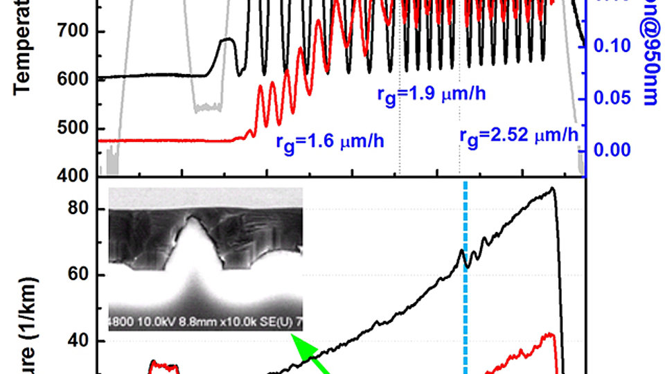
Distinct differences in stress development are apparent from the in-situ measured wafer curvature (Fig. 2). In spite of the typical tensile strain during growth of (0001) GaN on non-patterned sapphire, initial compressive stress is found when the lateral coalescence time is delayed on PSS. From the curvature measurement, the average compressive stress during (0001)-GaN layer growth on CPSS before coalescence is determined to be around 0.2 GPa. Subsequently, tensile stress comparable to growth on FSS builds up as soon as the surface is closed (Fig. 2, arrow). As a consequence, wafer curvature and in-plane residual stress can be controlled by changing the GaN coalescence speed depending on growth conditions and PSS properties.
While the (0001) c-plane orientation is the one currently used for LEDs, other orientations appear promising due to reduced polarization fields, but their growth is much more challenging. Therefore, the control of formation of semi-polar (11-22) and nonpolar (11-20) GaN phases on r-plane CPSS using different nucleation layer growth regimes has been investigated. With nucleation of GaN at low temperature (535°C) mainly semi-polar (11-22) GaN facets are formed. In contrast, increasing the nucleation layer temperature to 965°C, primarily (11-20) GaN is developed at 200 mbar. At reduced reactor pressure of 60 mbar, phase selectivity breaks down and semi-polar (11-22) and non-polar (11-20) GaN exist simultaneously. As a result, the crystalline quality of a-plane (11-20) GaN on r-plane CPSS can be effectively improved by means of optimized growth direction control.
Publications:
[1] M.-T. Wang, F. Brunner , K.-Y. Liao, Y.-L. Li, S.H. Tseng, M. Weyers, "Optimization of GaN wafer bow grown on cone shaped patterned sapphire substrates", J. Crystal Growth, vol. 363, pp. 109-112 (2013).
[2] M.-T. Wang, F. Brunner , K.-Y. Liao, Y.-L. Li, S.H. Tseng, M. Weyers, "Phase control of semi-polar (1122) and non-polar (1120) GaN on cone shaped r-plane patterned sapphire substrates", J. Crystal Growth, vol. 371, pp. 11-16 (2013).

