New in-situ analysis options for plasma etch processes at FBH
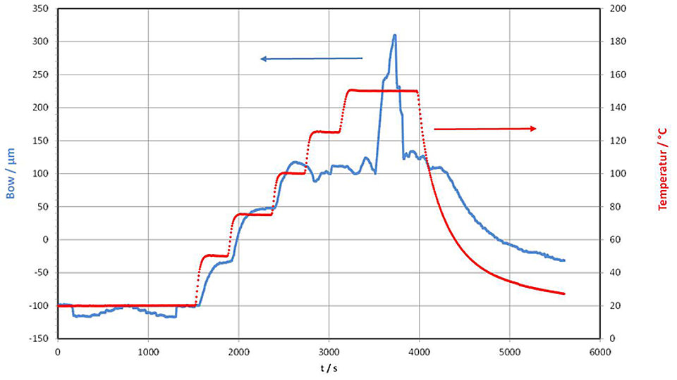
Fig. 2: Bow of a 100 µm thick SiC wafer glued to 1 mm sapphire, measured with EpiCurve system inside plasma reactor in dependence on temperature
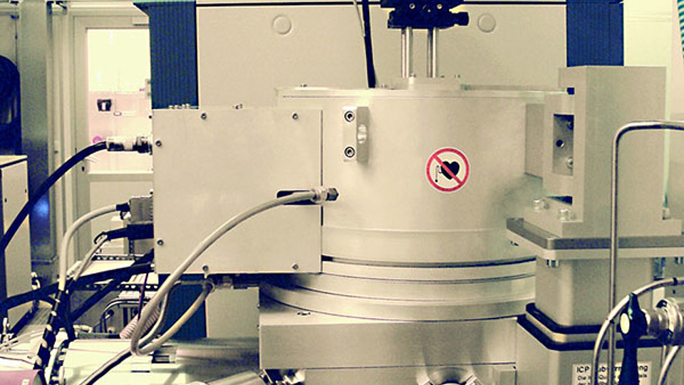
Dry chemical etching by means of highly reactive plasmas is one of the most important structuring methods in semiconductor industry. The materials that are being etched can be thermally stressed. This can result in deformation of the wafer which can affect the homogeneity and uniformity of the etch result and even lead to mechanical destruction of the wafer. Generally, deformations in an etch chamber cannot be observed directly. Now, FBH and the company Laytec succeeded in modifying one of the enterprise’s commercial sensors in such a way that allows determining the wafer bow (Fig. 1). For the first time, the impact of various process parameters on the bow of a wafer in a plasma etching chamber could be analyzed. Fig. 2 exemplarily shows the impact of the chuck temperature on the wafer bow.
The sensor was successfully applied to the optimization of process conditions during plasma etching of through-substrate vias (TSV) in 100 µm thick silicon carbide (SiC). Such thin materials are as flexible as paper and cannot be easily handled. Hence, they are temporarily glued to a supporting substrate and removed after processing. Performing a plasma etching process on a wafer - support wafer composite is a real challenge. In the etch chamber the composite is heated due to the etching process and also by a heating system, as the etch rates are higher at elevated temperatures. With the help of this sensor the etch parameters have been optimized in such a way that the bow caused by the process could be minimized, the process time decreased, and the yield increased. Selected aspects will be presented at the Compound Semiconductor Manufacturing Technology Conference CSMANTECH in May 2015.
Optimization of the etch process aims at further developing the processing of AlGaN /GaN HEMTs that are manufactured on SiC substrates. These components modulate the current with their gate from source to drain. A simplified mounting and hence a cost reduction becomes possible if all source contacts are in parallel and connected to the back side of the wafer. Vias are etched through SiC and AlGaN until a contact on the front side is reached and then filled with metal. Once the chip is soldered to its support an electrical contact is readily established. Now, a reduced number of bond wires is required which enables new and better design options. An example of such a contact is shown in Fig. 3. With this process optimization an important step towards further improving FBH’s mounting technology for AlGaN/GaN transistors could be achieved.
Publication:
A. Thies, W. John, S. Freyer, J. Beltran, O. Krüger, "Analysis and Optimization of a Through Substrate Via Etch Process for Silicon Carbide Substrates", CSMANTECH 2015, May 18-21, accepted for publication.
FBH research: 19.03.2015


