Ohmic backside contacts for blue-emitting laser diodes
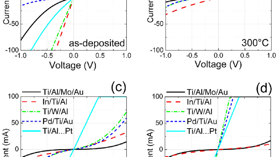
Fig. 1: Typical two-point I-V characteristics of various contact systems annealed at different temperatures.
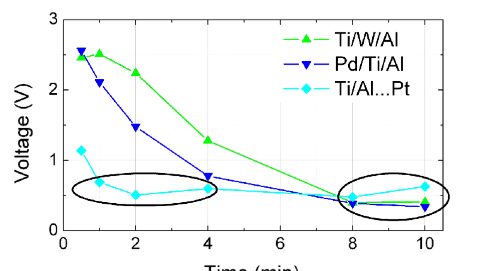
Fig. 2: Voltage at 90 mA measured in two-point geometry after annealing at 450°C. Circled points correspond to linear I-V characteristics.
The realization of custom-made laser diodes in the violet and blue spectral region is one of the focuses of the business area GaN optoelectronics at FBH. Narrow linewidth and single-mode external cavity diode lasers (ECDL) are developed for applications in sensing and bio-analytics (e.g. fluorescence spectroscopy), medical engineering and atom spectroscopy. When fabricating such laser diodes, the p-contact is usually made first on the epitaxial Ga-polar GaN(0001) surface and the n-contact is subsequently made on the N-polar backside of the previously thinned GaN substrate. However, this fabrication sequence is not compatible with the optimum annealing temperatures which are below 600°C for the p-contact (e.g. Pd) but beyond 800°C for the n-contact (e.g. Ti/Al/Mo/Au). Moreover, contact technologies for Ga-polar GaN surfaces can not be simply transferred to N-polar surfaces. Our studies have shown that the voltage drop at the backside contact is approx. 2 V during operation of a typical GaN ridge waveguide (RW) laser diode (chip size 0.4×0.6 mm2) if the laser is fabricated using the standard technology for the Ga-polar GaN surface. Therefore, we have developed a technology for ohmic contacts formation on the N-polar GaN surface which can be easily incorporated into the fabrication chain of a RW laser diode.
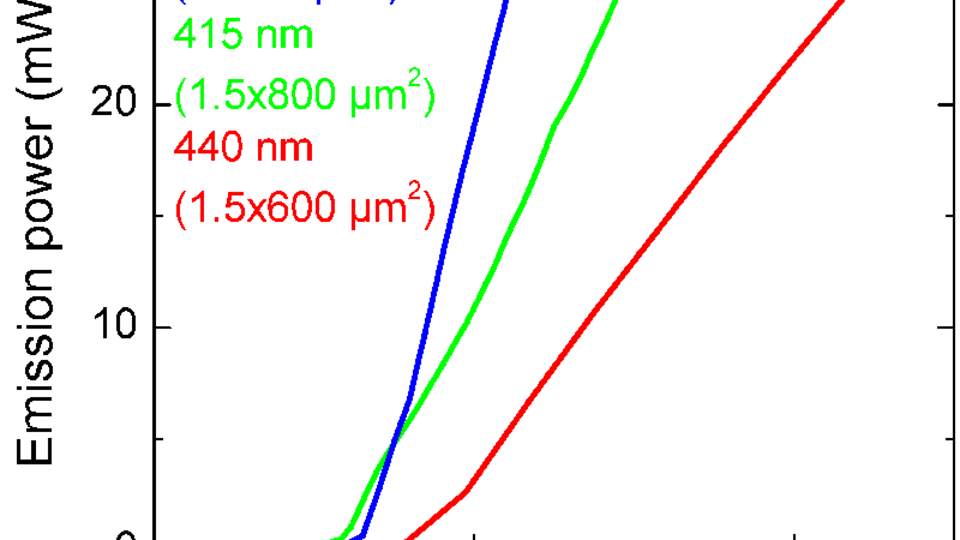
Various metal layer systems have been studied which are either based on literature data (In/Ti/Al, Ti/W/Al, Pd/Ti/Au) or an FBH’s long standing experiences with ohmic contacts (Ti/Al/Mo/Au, Ti/Al/Mo/Ti/Ni/Au/Ti/Pt). The contacts were fabricated on the lapped backside of GaN wafers and annealed at various temperatures. Figure 1 shows the I-V characteristics for different annealing temperatures. Some of the contact systems are ohmic even prior to any annealing but become highly resistive at the chip soldering temperature near 300°C. Three of the contact systems are linear after annealing at 450 to 500°C which is exactly in the targeted range between the soldering temperature and the optimum annealing temperature of the p-contact. Further studies were conducted to investigate the impact of the annealing time as shown on Fig. 2. As a result of this investigation we have now established the new metal system Ti/Al/Mo/Ti/Ni/Au/Ti/Pt for backside n-contact fabrication in GaN laser diodes. Figure 3 shows the L-I characteristics of such devices. Laser diodes with emission powers >20 mW in the wavelength range 405-440 nm can be fabricated reproducibly.
Publication:
Luca Redaelli, Anton Muhin, Sven Einfeldt, Peter Wolter, Leonhard Weixelbaum, Michael Kneissl "Ohmic Contacts on N-face n-type GaN after Low Temperature Annealing", accepted for publication in IEEE Photonics Technology Letters
FBH research: 30.04.2013


