Optimizing Multifinger Transistors for MM-Wave Power Amplification
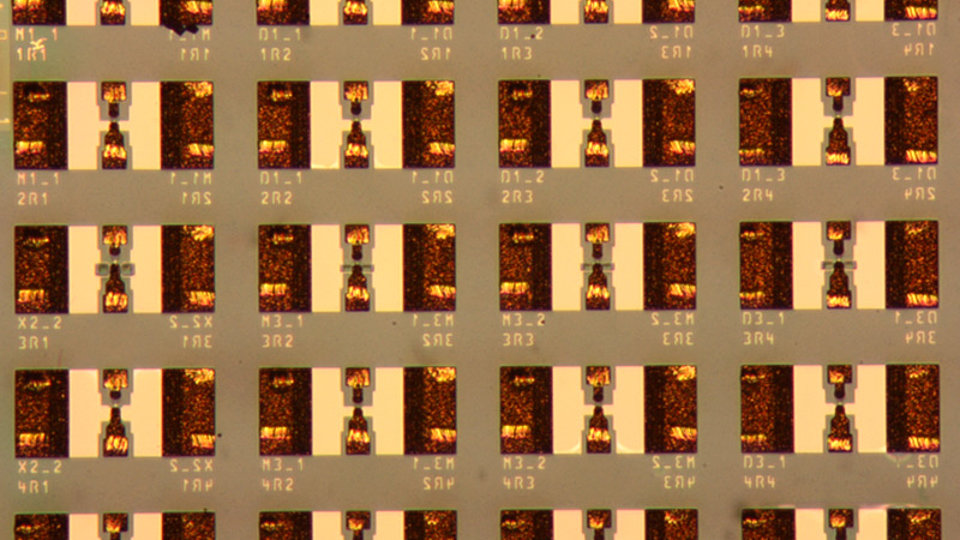
Transistor variations in TS-InP technology (upper pad is the base, lower pad is the collector, emitter is grounded)
To achieve higher output power levels of mm-wave power amplifiers, there are only a limited number of practical methods available. Heterojunction Bipolar Transistors (HBT) with sufficient gain at mm-wave or higher frequencies are restricted by the emitter size for a given technology. This limits the achievable output power per emitter finger. To increase the circuits overall power level it is then necessary to resort to power combining, which can be done on the circuit level by combining the outputs of different transistors, or on transistor level by increasing the number of fingers per transistors.
The last approach has the advantage that losses in the power combining network are avoided. The disadvantage is that parasitics, due to the necessary changes in transistor geometry, reduce the cut-off frequency as compared to the 1-finger transistor.
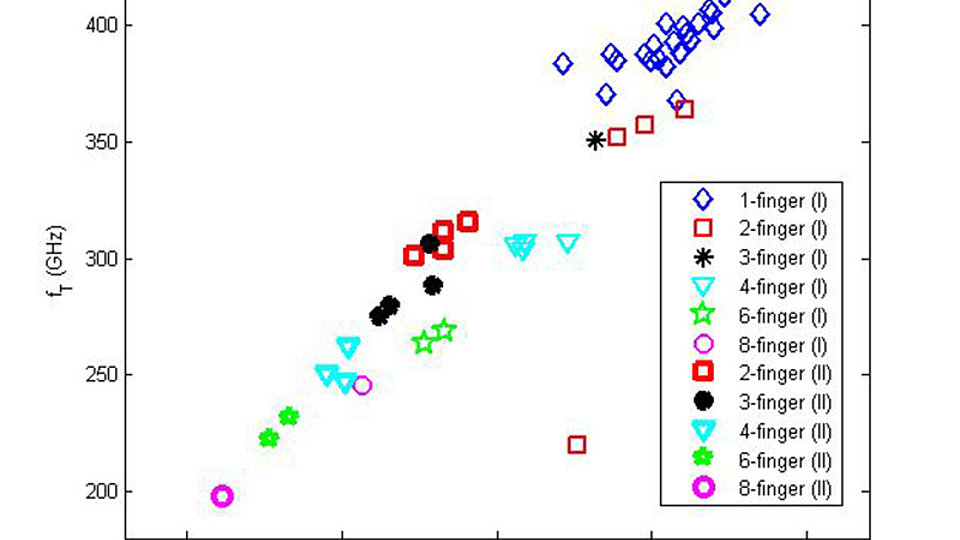
Work on multifinger transistors in FBH's Transferred-Substrate InP HBT technology has led to the development of 4-, 6-, and 8- finger transistors with transit frequency (fmax) values of 323, 283, and 256 GHz, respectively. Even though 1- and 2-finger transistors achieve approximately 375 GHz (the emitter finger size is in all cases 0.8 x 5 μm2). The realized multi-finger HBTs are suited for amplifier applications in the mm-wave range around 100 GHz. The top figure shows the short-circuit current gain cut-off frequency and the maximum frequency of oscillation for transistors with varying number of fingers. The figure shows two types of transistors (type I and type II) which exhibit an emitter area of 0.8 x 5 μm2 and 0.9 x 10 μm2, respectively. One clearly observes the general degradation in transit frequencies with increasing finger number, but within each group there are still differences that can be exploited to find the optimal transistor geometry.
Power measurements on matched amplifiers have indicated that the maximum output power level is 14-15 dBm@77 GHz (3.5 mW/μm2 emitter size) for a 2-finger transistor. This should allow almost 20 dBm output power for 8-finger transistors in the W band. At higher frequencies the number of fingers needs to be reduced or the emitter width must be downscaled.
The work is supported by DLR (Raumfahrt-Agentur, Deutsches Zentrum für Luft und Raumfahrt) under reference 50 RA 1103.
Publication:
T. Jensen, T. Kraemer, T. Al-Sawaf, V. Krozer, W. Heinrich and G. Tränkle , "Multifinger InP HBT’s in Transferred-Substrate Technology for 100 GHz Power Amplifiers", to be published at European Microwave Conference, Amsterdam, October 2012.
FBH research: 09.10.2012

