Patterning of 100 mm sapphire substrates for fabrication of semi-polar (11-22) GaN templates
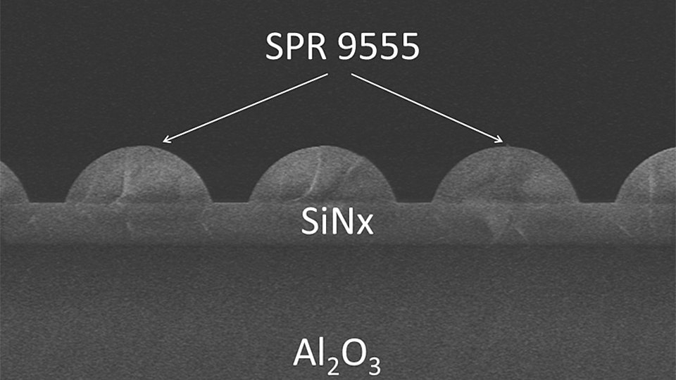
Fig. 1: Cross sectional scanning electron micrograph (SEM) of remelted photoresist SPR9555 on SiNx on r-plane sapphire
The FBH has recently developed a method to fabricate semi-polar (11-22) GaN on 100 mm diameter r-plane patterned sapphire (r-PSS). Such semi-polar GaN orientation can be utilized for the production of efficient light-emitting optoelectronic devices. While direct growth of non- or semi-polar GaN on planar sapphire is hampered by the incorporation of extended defects, the use of patterned substrates is promising. Here, the inclined growth in c-direction on the sidewall of trench-patterned r-oriented sapphire is particularly beneficial. To implement that, a reliable substrate patterning process had to be developed, since 4-inch r-PSS wafer are not commercially available. The FBH has developed a method to produce 100 mm diameter r-PSS by a combination of photolithographic and plasma etching methods.
Sapphire (Al2O3) is very resistant and chemically hard to etch, which makes patterning difficult. A dry etching process using inductively coupled plasma (ICP) combines a large ion energy with a high ion density, which is necessary to obtain a reasonable etch rate for sapphire. Since the r-plane surface of sapphire must be covered with SiNx during the epitaxial c-plane growth, SiNx was already used as masking material for plasma etching. The etching recipe was designed in such a way that a thin SiNx layer still remains as r-plane passivation at the end of the plasma processing.
The focus during sapphire structuring was on the creation of c-facets exhibiting an angle of approximately 58° to the surface normal. Due to the relatively high lattice energy of Al2O3 a defined etch angle is not readily achievable by optimizing the plasma etch conditions only. For materials with low lattice energy (for example Si or GaAs), the isotropy of the etching process and thus the side wall angle of the etched trenches can be controlled by the ratio of ion density to radical density. For materials with high lattice energy such an approach is not meaningful, because their surfaces are hardly attacked by radicals. Such materials can only be etched anisotropically using a dry chemical approach. In the reactive ion etching technique (RIE) employed at FBH the ions impinge vertically on the wafer surface. Therefore, slanted side walls in the sapphire can only be realized with etching masks already providing inclined side walls. The transfer of the slope angle of the etching mask into the substrate is determined by the ratio of the etching rates (etch selectivity) between masking material and substrate.
Positive photoresist (SPR9555) was used as an etching mask for dry chemical structuring of the r-plane passivation (SiNx). The resist was exposed using an i-line stepper, developed, and subsequently re-melted (Fig. 1). After optimizing the temperature and time of the resist reflow the side wall angle could be defined in the required manner. The pattern transfer from the photoresist to the SiNx film was performed by an anisotropic ICP etching process using SF6/He with an etch rate of 250 nm/min and an etch selectivity of about 1. After stripping the remaining resist the slanted pattern of the SiNx etching mask was transferred into the sapphire by a further r anisotropic ICP etching step using BCl3/Cl2/He with an etch rate of approximately 100 nm/min. Since the etch selectivity between SiNx and sapphire depends on various etching parameters, the resulting sapphire side wall angle could be controlled by adjusting the etch recipe. All dry etching processes were performed with an ICP plasma etch system of type SI 500 ICP from SENTECH GmbH.
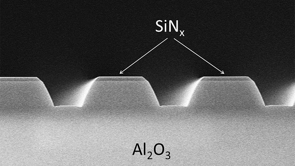
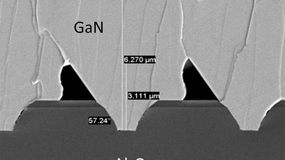
The cross section of the final r-PSS trench structure is shown in Fig. 2. The etched surfaces are very smooth and free of debris. The remaining SiNx passivation layer on the original r-plane is also visible. At FBH such patterned sapphire substrates were epitaxially overgrown (Fig. 3) and defect-reduced semi-polar (11-22) GaN templates could be successfully fabricated on 100 mm wafer scale for the first time.
Project: ALIGHT, EU FP7-NMP
Publication
F. Brunner, F. Edokam, U. Zeimer, W. John, D. Prasai, O. Krüger, M. Weyers, "<link publikationen pub18.htm _blank internal-url-new-window>Semi-polar (11-22)-GaN templates grown on 100 mm trench-patterned r-plane sapphire", phys. stat. sol. (b), vol. 252, no. 5, pp. 1189-1194 (2015).


