Simulation and design of compact tunable dual-wavelength diode laser systems
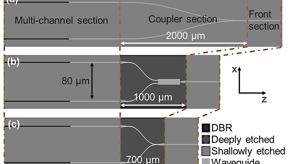
Fig. 1: Top view of different tunable dual-wavelength laser diode systems. (a) Reference design with a single etch depth, the novel designs (b) & (c) are based on two etch depths. (Note: different scales for lateral (x) and longitudinal (z) dimensions)
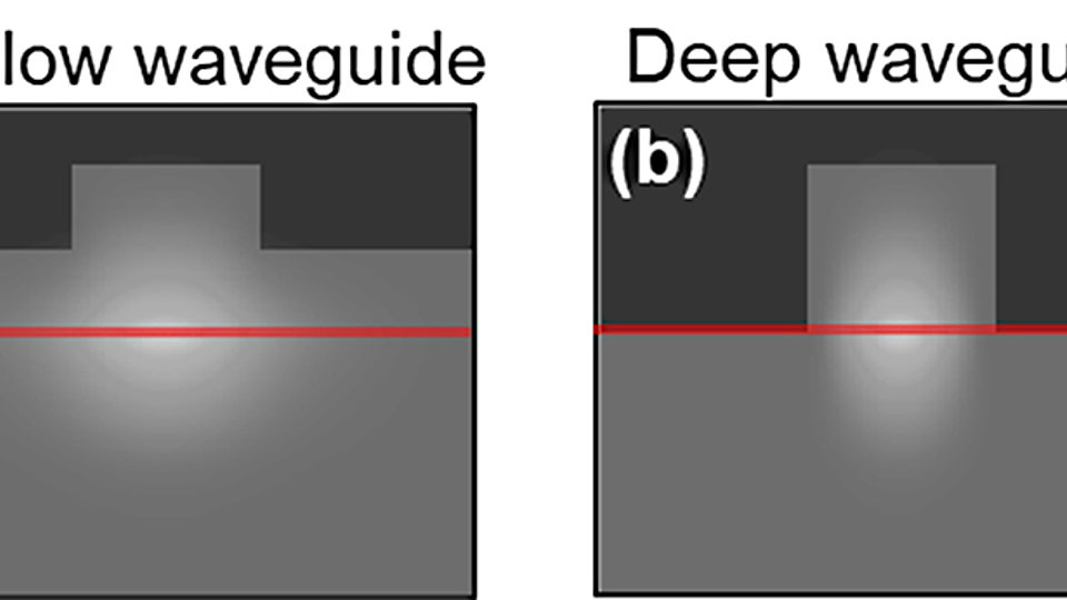
Fig. 2: Cross section of a shallowly (a) and a deeply (b) etched ridge waveguide - resulting fundamental mode is shown within each waveguide
Simultaneous emission of coherent light featuring two slightly detuned wavelengths out of one compact device is of interest for spectroscopic applications, namely absorption spectroscopy and shifted excitation Raman difference spectroscopy (SERDS). In addition, the ability of adjusting each of the emission wavelengths separately enables the generation of a tunable sum or difference frequency signal. For in situ measurements and portable solutions, compact laser sources with excellent spectral and spatial beam characteristics are inevitable – and therefore subject of intensive research at the FBH based on comprehensive simulations.
Dual-wavelength lasers can be realized by integrating two coupled laser channels, each equipped with a spectrally detuned and highly reflective distributed Bragg reflector (DBR) as shown schematically in Fig. 1 (a)‑(c). Both channels are coupled into a common front waveguide, resulting in a single light-emitting aperture. The lateral confinement of the optical wave inside the integrated waveguide components such as straight and bend waveguides are realized by etching parts of the chip surface and choosing appropriate contact layouts. The spectral fine-tuning of each laser channel is achieved by micro-heaters placed next to the DBRs.
In previous designs, the ridge waveguides were shallowly etched as shown in Fig. 2 (a), resulting in a 2000 µm long coupler section (see Fig 1 (a)). To reduce the coupler dimensions, we theoretically investigated a new design based on two etch depths, see Fig. 2 (a) and (b). Here, the regions where optical gain is supplied, namely the multi-channel and front section, indicated in Fig. 1, are shallowly etched to ensure fundamental lateral mode operation. In contrast, the coupler section is deeply etched to provide a higher refractive index contrast, enabling a more compact coupler section design having a length of 1000 µm and 700 µm for the devices shown in Fig. 1 (b) and (c), respectively.
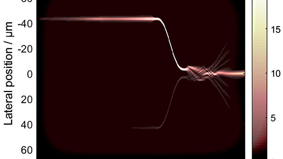
The device parameters of the integrated waveguide components, namely, S-bend, coupler and spot size converter were optimized using a numerically efficient simulation tool (FIMMPROP) for passive waveguides. Subsequently, the entire laser system was further analyzed applying the sophisticated traveling-wave equation based model WIAS-BALaser. Fig. 3 exemplarily shows the longitudinal-lateral (z,x) time averaged intensity distribution of the design shown in Fig. 1 (b) obtained by active BALaser simulations. In this specific case only the upper of two laser channels was electrically biased. It is visible that some of the forward traveling light got radiated behind the waveguide coupler. In addition, it can be seen that a part of the backward traveling wave is coupled into the lower unbiased laser arm. Those laser internal effects are neither accessible by passive simulations nor by experiments.
Following the introduced two etch depth design approach we reduced the coupler section length by at least a factor of two compared to previous results. In addition, it could be shown that active laser simulations are crucial to deduce critical and performance limiting design aspects not accessible otherwise.
Publication
J.-P. Koester, M. Radziunas, A. Zeghuzi, H. Wenzel, A. Knigge, "Simulation and design of a compact GaAs based tunable dual-wavelength diode laser system", Optical and Quantum Electronics 51(10), 334, (2019).


