Substrate mode suppression for an InP MMIC process
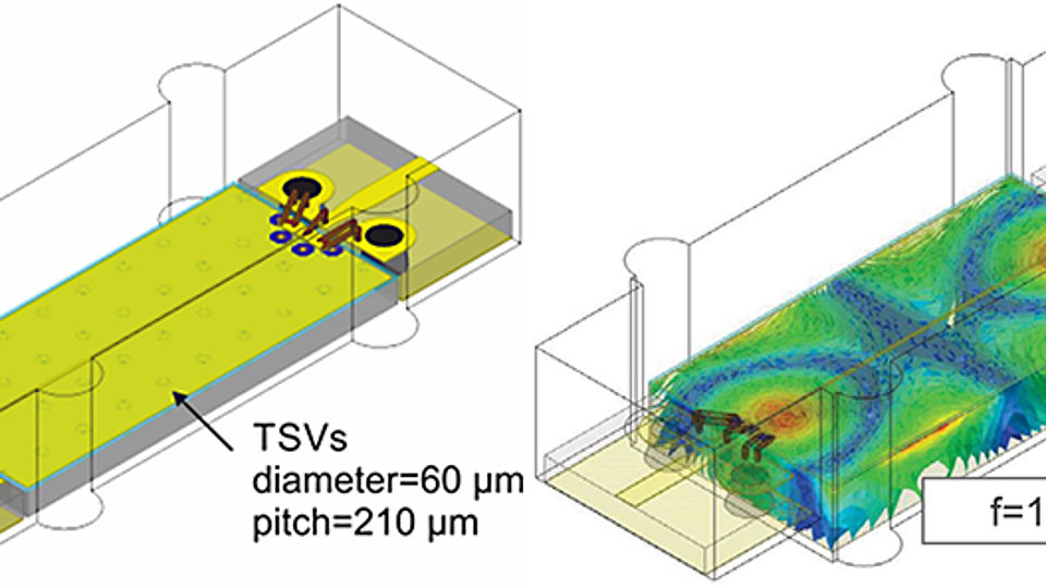
Fig. 1: Visualization of an alumina to MMIC bond wire transition (left) as used in EM simulation, showing the propagation of parasitic substrate modes when no TSVs are used. An example is given for 104.1 GHz (right).
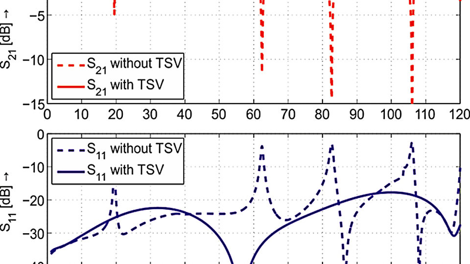
Fig. 2: Transmission S21 (blue) and reflection coefficient S11 (red) of alumina to MMIC bond wire transition with TSVs (solid) and without TSVs (dashed) from 3-D EM simulation.
Spearheaded by InP technology, the operational frequency of monolithic microwave integrated circuits (MMICs) reaches deep into the THz range. For increased operational frequencies undesirable modes can be excited in the circuit’s substrate, for example, by ground openings and by wire bond or flip-chip transitions as shown in Fig. 1 and Fig. 2. To ensure proper functionality of assembled modules and systems, substrate modes are commonly suppressed by thinning the substrate wafer and also by implementing through-substrate vertical-interconnect-accesses (TSVs). Since III-V materials are comparably fragile, these steps can be conducted more easily and reliably with silicon material.
Over the last years, FBH has developed an InP MMIC process in which the epitaxial layers are transferred from InP wafers to robust silicon host wafers [1]. The main advantages are higher cut-off frequencies due to fabrication of HBTs with reduced base-to-collector capacitances as compared to standard triple mesa transistors with the same transistor dimensions and due to wafer-level hetero-integration of InP DHBTs on silicon CMOS or BiCMOS technology [2]. Additionally, the transfer to silicon host wafers makes thinning and integration of TSVs straightforward [3].
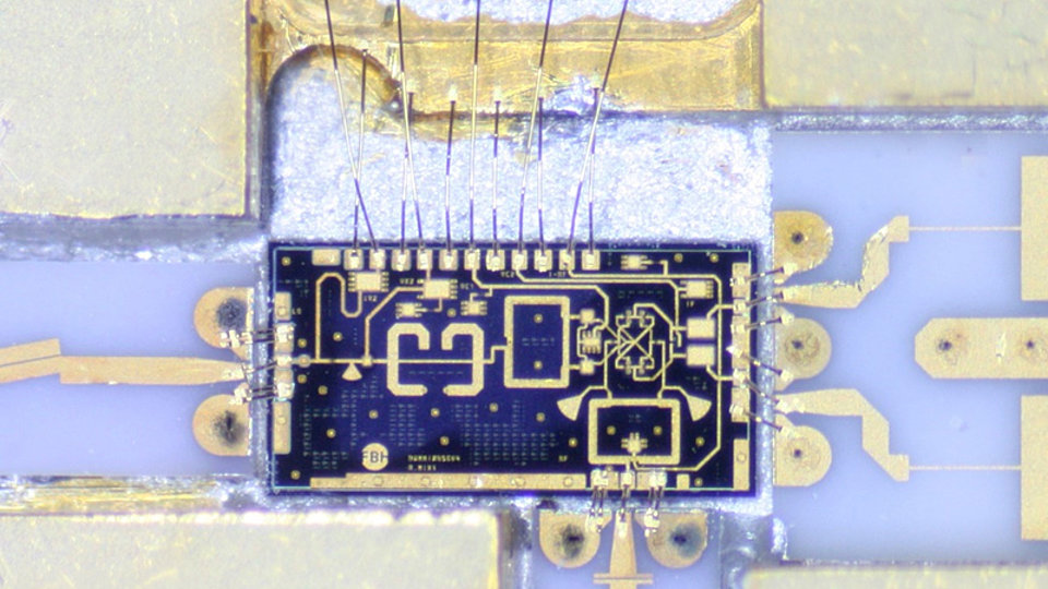
For FBH’s standalone InP process, TSVs and wafer thinning are introduced as standard module, relying on a "VIA first" process in TSV fabrication. First, intrinsic silicon wafers are patterned with alignment marks for wafer bonding of the transfer process. TSV are drilled with a nanosecond-pulsed UV laser operating at 355 nm. Via holes are electroplated with 10 µm of gold, filled with BCB and closed with metallic landing pads. Second, the transfer of epitaxial layers and the subsequent InP DHBT MMIC process is executed, including its 3 metal routing layers and its passive components. Finally, the silicon wafers are thinned to 127 µm and diced. Fig. 3 shows an InP MMIC with TSV for substrate mode suppression mounted and wire bonded in a 95 GHz radar module.
This work was supported in part by the DLR MIMIRAWE project by the Federal Ministry for Economic Affairs and Energy (grant number: 50RA1326). Further support was given by the Leibniz Association within the Leibniz Competition project THz InP HBT and by the European Commission within the Horizon 2020 program in the project Ultrawave.
Publications
[1] N. Weimann, D. Stoppel, M.I. Schukfeh, M. Hossain, T. Al Sawaf, B. Janke, R. Doerner, S. Sinha, F. J. Schmückle, O. Krüger, V. Krozer, W. Heinrich, M. Lisker, A. Krüger, A. Datsuk, C. Meliani, B. Tillack, "SciFab–a wafer‐level heterointegrated InP DHBT/SiGe BiCMOS foundry process for mm‐wave applications", physica status solidi (a) 213.4, 909-916 (2016).
[2] N. Weimann, T. Johansen, D. Stoppel, M. Matalla, M. Brahem, K. Nosaeva, S. Boppel, N. Volkmer, I. Ostermay, V. Krozer, O. Ostinelli, C. Bolognesi, "Transferred substrate InP/GaAsSb heterojunction bipolar transistor technology with fmax > 0.53 THz", IEEE Transactions on Electron Devices 65.9, 3704-3710 (2018).
[3] D. Stoppel, M. Hrobak, A. Külberg, S. Schönfeld, D. Rentner, O. Krüger, K. Nosaeva, M. Brahem, S. Boppel, N. Weimann "Through silicon via (TSV) process for suppression of substrate modes in a transferred-substrate InP DHBT MMIC technology", Proceedings of Compound Semiconductor Week 2018, p. 59 (2018).


