Thermal characterization of AlGaN/GaN HEMTs on Si and n-SiC substrates
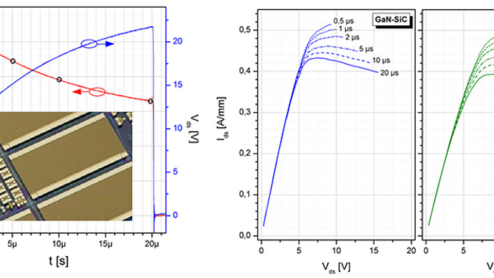
Fig. 1: Pulsed IV characterization of large periphery devices fabricated on SiC and Si substrates; single pulses (l.), I-V characteristics taken for different pulse durations (r.)
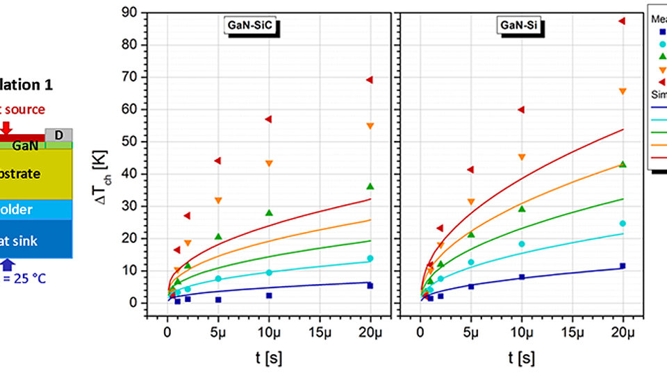
Fig. 2: Schematic of heat source for device operation in linear region (l.); difference channel - baseplate temperature for GaN on SiC and Si substrates (m. and r.)
Channel temperature characterization of AlGaN/GaN devices is an important feature for reliability estimation and assessment of power switching losses. We present here a method to thermally characterize large AlGaN/GaN HFETs based on pulsed electrical measurements. The thermal properties of large periphery 60 mΩ AlGaN/GaN HEMTs (214 mm gate width, 134 gate fingers) fabricated on Si and SiC substrates have been studied by applying pulsed Ids characterizations at varying base plate temperatures, subsequently correlating it to ANSYS simulations.
The pulsed measurements have been performed at TU Berlin on a special setup capable to handle drain current levels up to 200 A. This measurement system has been developed in the frame of the Joint Lab Power Electronics, a cooperation between TU Berlin and FBH. For the actual measurements, devices are pulsed to any bias point in the output I-V characteristics (Vds = 0…20 V) for a constant pulse length of 20 µs. The time dependency of the drain current during the pulse is monitored with very high time resolution. The dynamic Ids-Vds characteristics were then extracted from these data sets at various time points (for example at 0.5, 1, 2, 5, 10 and 20 µs after the switching event, see Fig. 1). The branches of the output characteristics were probed at isothermal conditions to calibrate the measurement routine by applying very short pulses of 0.5 µs duration only at different base-plate temperatures.
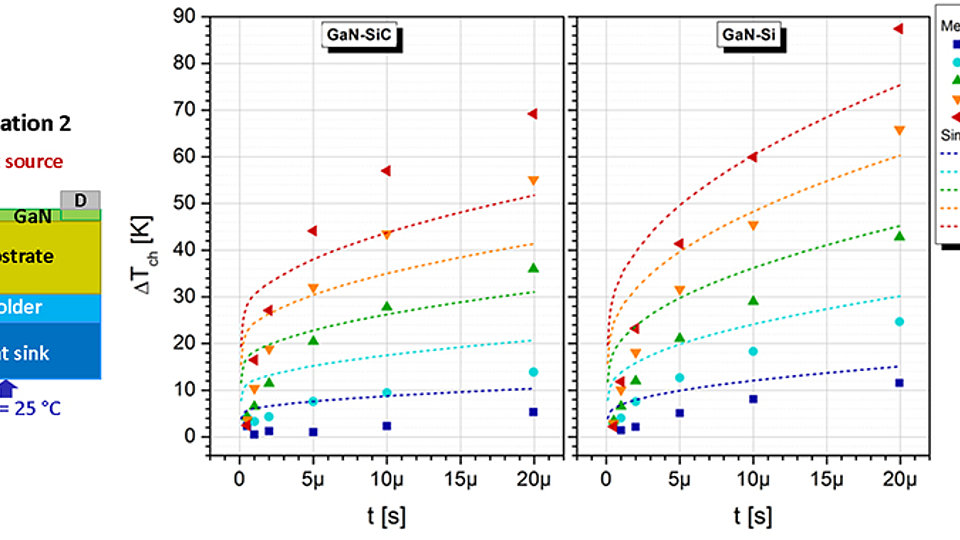
The experimental results have then been compared to thermal transient simulation (ANSYS) of idealized GaN-on-Si and GaN-on-SiC structures for two heat source configurations (see Figs. 2 and 3). Simulation bases on a simplified 1-finger model with boundary conditions adjusted to the thermal properties of fingers in the center of the large periphery transistor. Depending on whether the devices are operating in the linear or the saturation region the heat source has been defined as an area between source and drain contact (simulation 1, Fig. 2) or an area close to the drain side edge of the gate (simulation 2, Fig. 3), respectively.
As expected from the differences in thermal conductivity of SiC and Si substrates, devices on Si substrate show a higher channel temperature as compared to GaN-on-SiC devices. This applies if the pulse duration increases and if the device is biased in the saturation region. However, at bias points being typical for power switching (linear region of I-V characteristics) the thermal properties of devices on SiC and Si are fairly comparable. In the linear region, simulation 1 matches very well to the experiment (see Fig. 2, branches with 1 and 2 W/mm). In this case, the assumption of the heat source distribution in the device is valid. The more the device is operated towards the saturation region, the more the heat source shifts to the drain side edge of the gate, which means that for predicting the thermal properties of the saturated device simulation 2 (Fig. 2) becomes valid. Indeed, for the saturated device the now modified heat source distribution provides the better matching to the experiment (see Fig. 3).
Publication:
R. Zhytnytska, J. Böcker, H. Just, E. Bahat-Treidel, O. Hilt, S. Dickerhoff, J. Würfl, G. Tränkle, "Thermal characterization of AlGaN/GaN HEMTs on Si and n-SiC substrates", To be published in Proceedings Int. Conf. on Compound Semiconductor Manufacturing Technology (CS ManTech 2015).
FBH research: 02.04.2015


