Trap characterization of GaN HEMTs with MHz load-line measurements
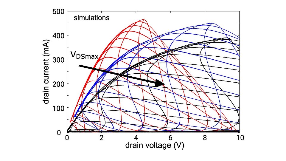
Fig. 1: Simulations of MHz load-lines varying maximum drain voltage (VDS) to progressively achieve stronger trapping effects. The increased Ron and the current collapse can be seen on the reduced current at the upper edges of the load-lines.
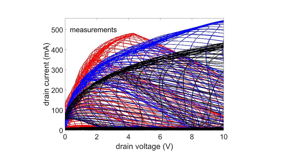
Fig. 2: Measurements of MHz load-lines. As predicted by the model, knee walkout and current collapse are again observed when the maximum drain voltage (achieved by the load line) is increasing.
Gallium nitride (GaN) high electron mobility transistors (HEMTs) represent the forefront of technology for high-power and high-frequency applications. Their superior power capabilities and low noise figures facilitate efficient and compact integration into full GaN RF front-end modules, thereby minimizing costs and system size. Precise compact models are indispensable for achieving accuracy on such designs. However, they must consider various nonideal phenomena in GaN HEMTs, including trapping effects [1].
Trapping effects, which occur during high voltage and high-power operations, can reduce drain current (IDS), output power, and device efficiency. This makes accurate characterization and comprehension of these effects crucial – not only for model precision but also for technological optimization. Pulsed current-voltage measurements are a common characterization technique for this purpose, however, they often prove time-intensive, complex, and require expensive equipment.
At FBH, in cooperation with BTU Cottbus-Senftenberg in the Joint Lab BTU−CS − FBH Microwave, we have developed an innovative characterization technique for trapping effects in GaN HEMTs [2]. This method involves the deliberate interference of two waves within the device, generating a complex set of current-voltage (I-V) trajectories. These trajectories initially fill traps with electrons, inducing trapping effects, and subsequently cover the entire I-V plane to produce I-V characteristics suitable for analysis and device modeling. These measurements are relatively rapid, can be performed with low-cost equipment, and reflect real-world conditions.
A set of these trajectories, obtained from simulations, is illustrated in Fig. 1. The simulations facilitated the development of the final measurement setup. The goal is to manipulate the setup to produce curves with varying magnitudes of trapping. Key factors influencing these curves include the maximum load-line drain voltage, VDSmax. As VDSmax increases, more traps are filled with electrons, causing current collapse and knee walkout as observed in Fig. 1, predicted by the model. The reduction of current in the upper region of the I-V plane as VDSmax increases is responsible for power and efficiency degradation in power and low noise amplifiers.
The proposed setup has been implemented and evaluated with actual measurements on FBH GaN HEMTs. A set of these measurements is presented in Fig. 2, where different colors represent different VDSmax values and, consequently, different trap states. The predicted current collapse and knee walkout are reproduced by the measurements, demonstrating excellent agreement and promising potential for trap models and optimization analysis.
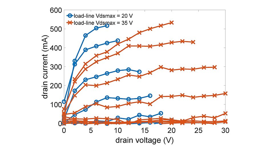
To further enhance the utility of these measurements, we developed a tool to derive common output or transfer I-V characteristics from these trajectories. Through interpolation within the measured IDS-VDS-VGS plane, we created I-V curves, as shown in Fig. 3. For simplicity, we compare two cases: one measurement with VDSmax = 20 V and another with VDSmax = 35 V. These curves are invaluable for trap model parameter extraction or evaluation of trapping effects. Models extracted from such I-V curves, which encompass a wide range of trap states, can simulate device performance with high accuracy [1]. By utilizing MHz load-line measurements, we streamline the model's requirements, reducing both time and cost while maintaining precision.
This work was financially supported by Deutsche Forschungsgemeinschaft (DFG) under grant no. RU 1203/16-1, and partially funded by the German BMBF within the ”Forschungsfabrik Mikroelektronik Deutschland (FMD)” under ref. 16FMD02.
Publications
[1] P. Beleniotis, S. Krause, C. Zervos and M. Rudolph, "A Physics-Based Model for Slow Gate-Induced Electron Trapping in GaN HEMTs," in IEEE Transactions on Electron Devices, vol. 71, no. 7, pp. 4058-4065, July 2024, doi: 10.1109/TED.2024.3397234.
[2] M. Rudolph, P. Beleniotis, C. Zervos, U. L. Rohde and C. Andrei, "Determining GaN HEMT Trap Models from MHz Load-Line Measurement – A Case Study," 15th German Microwave Conference (GeMiC), Duisburg, Germany, 2024, pp. 29-32, doi: 10.23919/GeMiC59120.2024.10485297.


