3-dimensional integration of SiGe-BiCMOS and InP-HBT technology
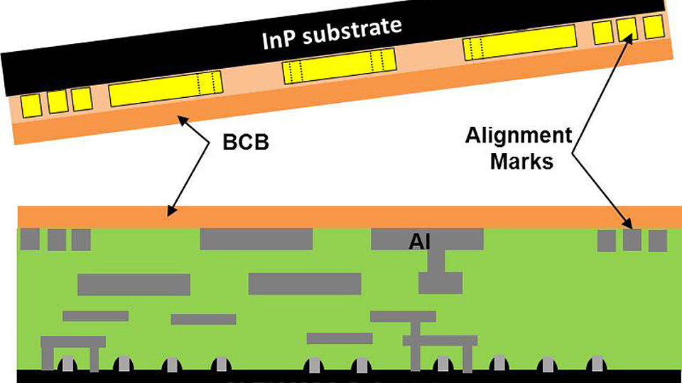
Fig. 1: The separately processed InP and SiGe-BiCMOS Wafers are adjusted by capable alignment marks and bonded using BCB with an accuracy better than < 10 µm.
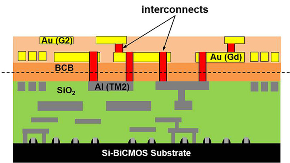
Fig. 2: After the wafer bond process, the InP substrate is removed, and the structures processed before are exposed. The interconnects between InP and Si technology are formed by dry etching and plated with gold.
Indium Phosphide (InP) Hetero-Bipolar Transistor (HBT) high frequency circuits fabricated at FBH by far exceed the performance of silicon devices in terms of RF power and frequency range. Due to its high electron mobility and breakdown voltage, InP technology opens up application fields that are difficult to access with RF-CMOS and SiGe-BiCMOS technology. The capability to generate high RF power at high frequencies enables millimeter wave imaging applications, e.g. high-resolution radar systems and terahertz scanning. Also, for future wireless communication systems with data rates exceeding 100 Gbit/s, amplifiers and mixers in InP Technology operating at 300 GHz and above are key enabling components.
Silicon is the dominating material of modern semiconductor technology with a market share of 98,5%. Established process modules, high integration density and yield enable a cost-efficient production of integrated circuits with high complexity. However, as application frequencies rise above 100 GHz, the limited RF power performance of silicon-based circuits at these frequencies becomes a bottleneck.
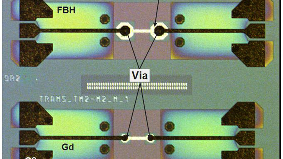
In order to profit from the advantages of both technologies, InP and silicon, the joint "HiTeK" project funded within the SAW context. FBH and the Leibniz Institute for Innovative Microelectronics (IHP) aim to establish a technology platform for heterogeneous integrated circuits at terahertz frequencies (0,1-1 THz) [1]. Within this project, the established InP HBT transfer-substrate-process at FBH [2], is combined with IHP's Silicon-Germanium BiCMOS process. First, InP and silicon wafers are processed separately at FBH and IHP, respectively. Since IHP's production line uses a wafer size of 200 mm in diameter, the wafers need to be cut into 3" diameter wafers for compatibility with FBH's process line. Utilizing benzocyclobutene (BCB) based wafer bonding, the 3-dimensional integration of both technologies is performed at FBH (see fig. 1). In order to meet the requirements for lateral wafer-to-wafer alignment accuracy of less than 10 µm, the wafer bond process has been improved for the new materials system InP/BCB/Si. After wafer bonding, the InP substrate is completely removed, and the previously created structures in InP and BiCMOS technology are exposed (see fig. 2). By dry etching, short and thus low-impedance vertical interconnects (vias) are defined between InP and Si-BiCMOS. Within the BiCMOS technology, aluminum is used as an interconnect metal. Since aluminum tends to form an oxide passivation layer which could increase the contact resistance of the vias, special attention needs to be focused on the via process. By optimizing the fabrication procedures, via resistance decreased from multiple ohms down to 300 mOhm. In a first technology run, passive microstrips have been tested which were designed in accordance to the given requirements. The test structures consist of gold transmission lines on the InP side, two via transitions in and out of the silicon circuit layers, and an aluminum transmission line on the silicon side. The propagation loss in the gold transmission line on the InP side amounts to 0,4 dB/mm. We can therefore extract a loss of 0,36 dB per via. The low loss and the attained frequency behavior are matching well with the simulation. This result is a first proof of the monolithic high-frequency integration of our InP-HBT and SiGe-BiCMOS technologies. Wafers with active circuits are currently being processed and are expected to be completed in the coming months.
Publications:
[1] M. Lisker, A. Trusch, M. Fraschke, P. Kulse, Y. Borokhovych, B. Tillack, I. Ostermay, T. Krämer, F.J. Schmückle, O. Krüger, V. Krozer, W. Heinrich, "InP-Si BiCMOS Hetero Integration for Broadband Radio Links", submitted to Smart Systems Integration, International Conference & Exhibition, 2013.
[2] T. Kraemer, M. Rudolph, F.J. Schmueckle, J. Wuerfl, G. Traenkle, "InP DHBT Process in Transferred-Substrate Technology With ft and fmax Over 400 GHz", IEEE Transactions on Electron Devices, Vol. 56 (9), p. 1897 – 1903, 2009.
FBH research: 06.11.2012


