A new technological platform for red emitting DFB lasers with surface gratings
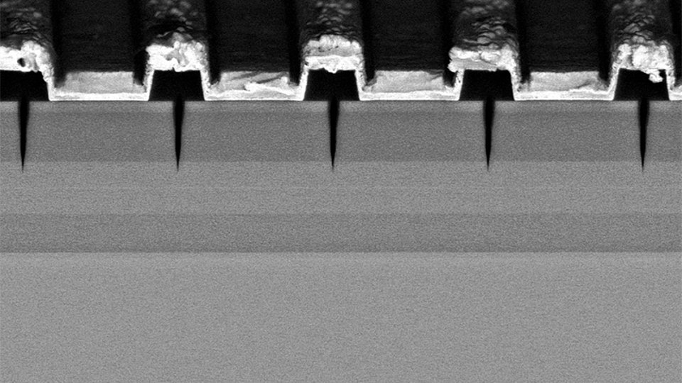
Fig.1. Scanning electron microscope picture of a Bragg grating with etched and encapsulated grooves.
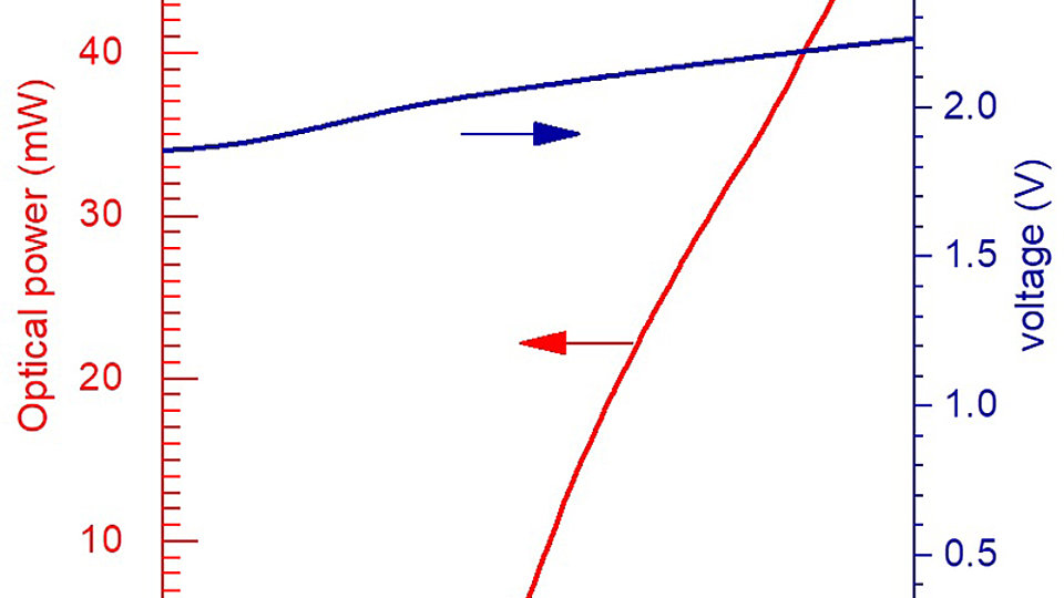
Fig. 2. Continuous-wave output power (left axis) and applied bias (right axis) versus injection current of a 1.5 mm long DFB laser.
Applications in holography, spectroscopy and medicine need lasers that provide an ultra-small optical spectrum, which can be not be achieved by common Fabry-Perot type of diode lasers. Instead, Bragg gratings have to be employed – periodic variations of the refractive index along the cavity axis fixing the lasing wavelength. They can either be implemented in only a part of the cavity being electrically unbiased (distributed Bragg reflector, DBR, laser) or along the whole cavity containing both the laser-active region and the grating (distributed feedback, DFB, laser). DBR lasers can be fabricated more easily but suffer from wavelength jumps and show self-pulsating behavior when current or temperature is varied. On the other hand, DFB lasers exhibit a spectrally and temporally more stable behavior but are more difficult to fabricate, because the gratings are commonly embedded into the epitaxial layer structure employing a two-step epitaxy. This is especially true for lasers containing the semiconductor AlInGaP with emission in the wavelength range between 630 nm and 690 nm.
Therefore, FBH’s well proven surface grating technology to fabricate DBR lasers was adapted to DFB lasers. Surface gratings are realized by etching narrow grooves deep into the completed epitaxial layer structure so that no re-growth is necessary. For DBR lasers, typically gratings with Bragg orders in the range between 3 and 10 are used, resulting in grating periods between 0.3 and 1 µm. Utilized in a DFB laser, the small spacing of the etched grooves would hinder the injection of the electrical current into the cavity, containing both the laser-active region and the grating. Therefore, 40th order Bragg gratings with a period of 4 µm were used. The now much larger distance between the grooves can be easily metallized so that a homogeneous current injection can be achieved along the whole cavity.
To accomplish this, a three layer system consisting of a baked resist, Ti and an electron beam resist is exposed by electron beam lithography (VISTEC SB251) and further patterned with an O2 plasma. The obtained grating is then transferred into the semiconductor layers via reactive ion etching (RIE). The etch depth of the grooves has to be carefully adjusted to achieve an appropriate feedback strength. Furthermore, the grooves must be at least a few tens of nm wide at the bottom to obtain low scattering losses. This is realized by choosing a proper opening of the resist and a tailored etching process to realize V-shaped grooves, see Fig. 1. After etching the ridge waveguides (RWs) for lateral optical confinement, electron beam lithography and similar processing steps as mentioned before were applied to encapsulate the etched grooves by SiN, see Fig. 1. This allows keeping the serial resistance of the device comparable to lasers without gratings.
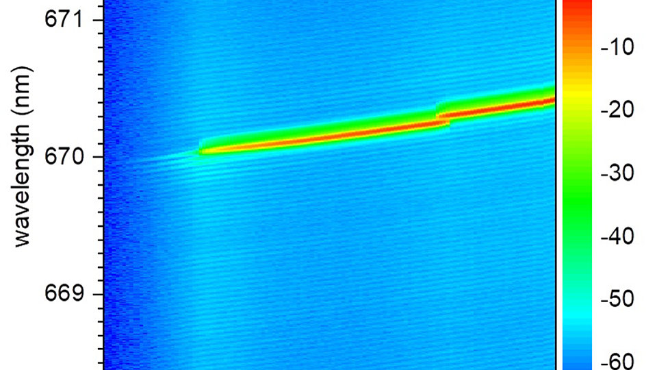
The fabricated lasers emitting around 670 nm achieved 50 mW output power at an injection current of 180 mA (Fig. 2). A color-scale mapping of the optical spectrum versus injection current indicates single-mode operation over a wide current range with only one mode hop at 150 mA (Fig. 3). The side modes are suppressed by more than 50 dB.
The successful demonstration of 670 nm RW DFB laser operation has proven the effective development of a new technological platform, which can be used to fabricate similar lasers emitting at a multitude of other wavelengths.
Publications
V. Z. Tronciu, H. Wenzel, M. Radziunas, M. Reggentin, J. Wiedmann, A. Knigge, “Investigation of red-emitting distributed Bragg reflector lasers by means of numerical simulations”, IET Optoelectron. vol. 12 (5) pp. 228-232 (2018)
J. Fricke, O. Brox, H. Wenzel, M. Matalla, P. Ressel, and A. Knigge, “Red-emitting distributed-feedback ridge-waveguide laser based on high-order surface grating”, Electron. Lett., vol. 54 (9), pp. 582-583 (2018)


