Accelerated on-state stressing of normally-off GaN transistors for power switching applications
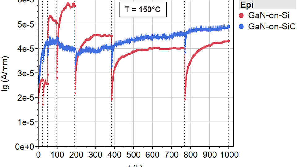
Fig. 2. Gate current transient of GaN-on-SiC (blue) and GaN-on-Si (red) transistors during 1000 h stressing. Measurement was interrupted for DC characterization (dashed line)
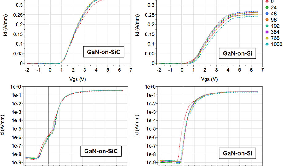
Fig. 3. Evolution of DC transfer characteristics for GaN-on-SiC (l.) and GaN-on-Si (r.) transistors during 1000 h stressing in linear (top) and logarithmic scale (bottom). Vds = 10 V
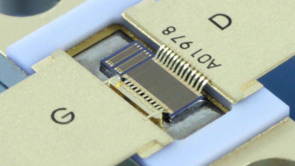
GaN-based high-voltage power switching transistors enable efficient power converters with increased power density due to the low area-specific on-state resistance for a given blocking strength and the low switching losses. Normally-off operation is a precondition for power electronics. Thus, FBH has chosen the p-GaN gate approach. Here, the gate is a junction between the p-doped GaN gate and the n-type GaN transistor channel, separated by an AlGaN barrier which shows pin-diode characteristics. Competing approaches for GaN-based GaN HFETs use either a Schottky-type metal gate, also with diode characteristics, or an electrically insulating gate with a dielectric in between the gate metal and AlGaN barrier.
Much work has been done in the past to study device reliability of GaN-based HFETs under different operation conditions, in particular under off-state stress with high drain bias. In an additional study, FBH now focused on the on-state stress of p-GaN gate normally-off devices. In transistor on-state conditions with 5 V applied to the gate, the pin gate diode carries a small forward current, and any related aging effects will differ from the issues observed in the competing GaN HFET approaches with either Schottky-type or MIS-type gate modules.
Test transistors with 3.2 mm gate width were set to typical on-state conditions for switching application. For 1000 h, the gate was biased with 5 V, and a drain current of 50 mA/mm was realized by biasing the drain to approximately 1.5 V. The ambient temperature was set to 150°C to accelerate any aging effects. DC device characteristics were taken at the beginning and at the end of the stress and at six intermediate intervals. Transistors with different epitaxial (Al)GaN stacks on either SiC or Si substrate were tested.
The gate current during stressing doubles in the first 50 hours for both epitaxy stacks. The gate current increases by another 25% for the GaN-on-SiC device when stressed up to 1000 h. In contrast, strong fluctuation is seen for the GaN-on-Si transistor. It takes around 100 h after all intermediate cool-down periods for the DC characterization before the equilibrium gate current is re-established. This indicates for charge trapping at the pin junctions. Off-state drain leakage, threshold voltage, and maximum drain current are not affected by the 1000 h stressing sequence for the GaN-on-SiC transistor. A threshold voltage shift of +0.3 V (in the first 24 h) and a drain current reduction of 11% during the whole stressing period was observed for the GaN-on-Si device.
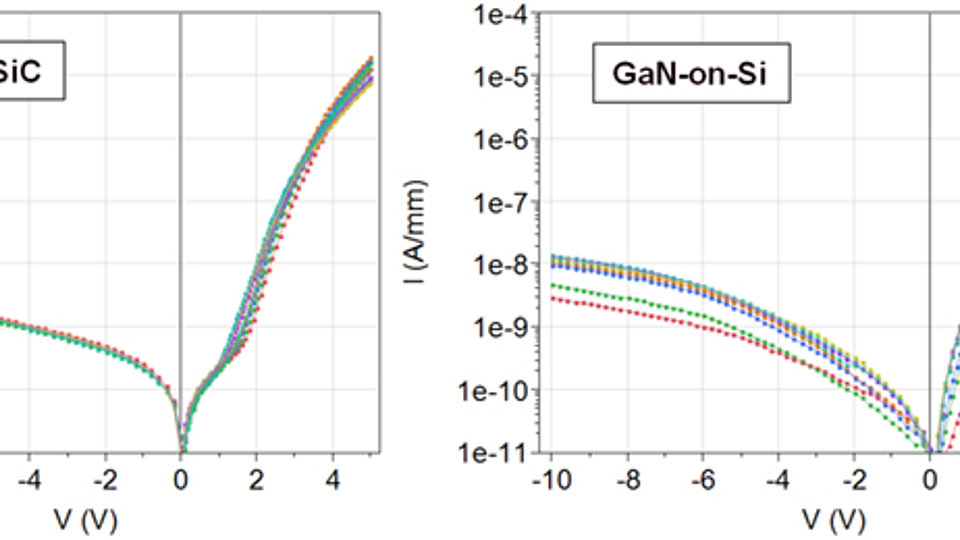
Principal differences between both devices were detected for the gate diode. The gate current for 1 V gate bias increases for the GaN-on-Si device by a factor of 30 in the first 96 h, but only a 50% increase during the full 1000 h stressing period has been observed for the GaN-on-SiC transistor. The reduced blocking capability of the GaN-on-Si gate diode is also reflected in the 5 times increased reverse leakage at -10 V.
In conclusion, 1000 h on-state gate stressing at 150°C has been performed on normally-off p-GaN gate transistors to check for reliability of this novel gate module. The interface quality of the GaN-channel, AlGaN barrier, and p-GaN epitaxial layers is of significance for stable gate-diode performance. Gate-diode degradation results in threshold voltage shift and drain current reduction. The GaN-on-SiC technology showed no degradation and is therefore suited for power electronics.
Publications:
O. Hilt, E. Bahat-Treidel, A. Knauer, F. Brunner, R. Zhytnytska, J. Würfl, "High-voltage normally OFF GaN power transistors on SiC and Si substrates", MRS Bull., vol. 40, no. 05, pp. 418-424 (2015).
M. Ťapajna, O. Hilt, E. Bahat-Treidel, J. Würfl, and J. Kuzmík, "Investigation of gate-diode degradation in normally-off p-GaN/AlGaN/GaN high-electron-mobility transistors", Appl. Phys. Lett., vol. 107, no. 19, pp. 193506 (2015).


