Advancing on-wafer measurement calibration at W-band
In the research and development of integrated circuits it is necessary to measure the circuits before dicing. Those measurements are carried out with the help of measurement needles, so-called probes. Applying these probes means to generate additional parasitic effects deteriorating the real physical result. Undesirable parts need therefore to be removed from the measurement result. To achieve this, the FBH works together with the American National Institute of Standards and Technology (NIST) and the German Physikalisch-Technische Bundesanstalt (PTB) on improving and refining the correction algorithms for the calibration in the high frequency range.
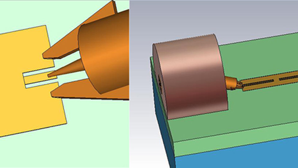
Fig. 1 shows examples of a measurement set-up with probes and a simple coplanar test circuit (shorted CPW). The prober pads, as well as the probe itself, generate additional electromagnetic effects, as for example field and wave coupling, which increase with frequency. To compensate these effects a calibration is executed which shall correct the measurement result of a circuit (Device Under Test = DUT) by the effects attributed to the probe. The calibration process, in turn, needs measurement results of a series of test lines (lines of varying length and terminations). The test structures have to be processed in the same technology and probed in the same environment in order to contain the same parasitic effects as the DUT. In the direct vicinity, for example, there should be the same neighboring structures, if any. Furthermore, the calibration process assumes single-mode propagation which, in general, is not the case.
Also, repeated measurements show additional scattering in data. The reasons are manifold and include deviations in measurement equipment as well as in wafer chuck and various mechanical tolerances (force onto the needles, angle, probe offset). The consequence of all these uncertainties is that deviations grow and errors increase with frequency significantly.
The cooperation between FBH, NIST, and PTB aims at detecting and identifying the parasitic effects in order to improve the correction algorithm in the calibration. In a first step, investigations were carried out to define and understand the parasitic effects and radiation properties. Extensive electromagnetic simulations were performed, taking each detail into account, especially the probe geometry. The results of these simulations show a good agreement with the measurement results.
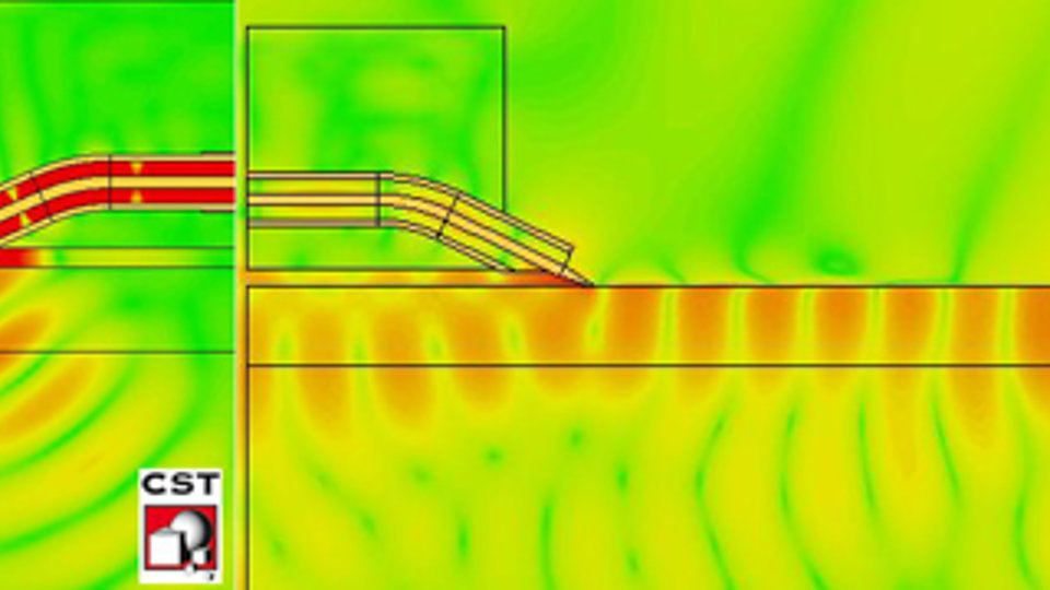
Analyzing the electromagnetic fields most of the physical phenomena occurring during measurements have been identified and can be explained, particularly the various types of coupling and radiation (Fig. 2). However, a full quantitative description is still missing, which could be implemented into the correction algorithm. In order to achieve this, some open questions need yet to be resolved, as for example the issue of reproducibility for different DUTs and to which degree inevitable inaccuracies will deteriorate the measurement results, even with an improved correction algorithm.
Publication:
D.F. Williams, F.-J. Schmückle, R. Doerner, G. N. Phung, U. Arz, W. Heinrich, "Crosstalk Corrections for Coplanar-Waveguide Scattering-Parameter Calibrations", IEEE Transactions on MTT, accepted for publication (2014).
FBH research: 01.07.2014

