AlGaAsP strain compensation layers in GaAs-based edge emitting diode lasers
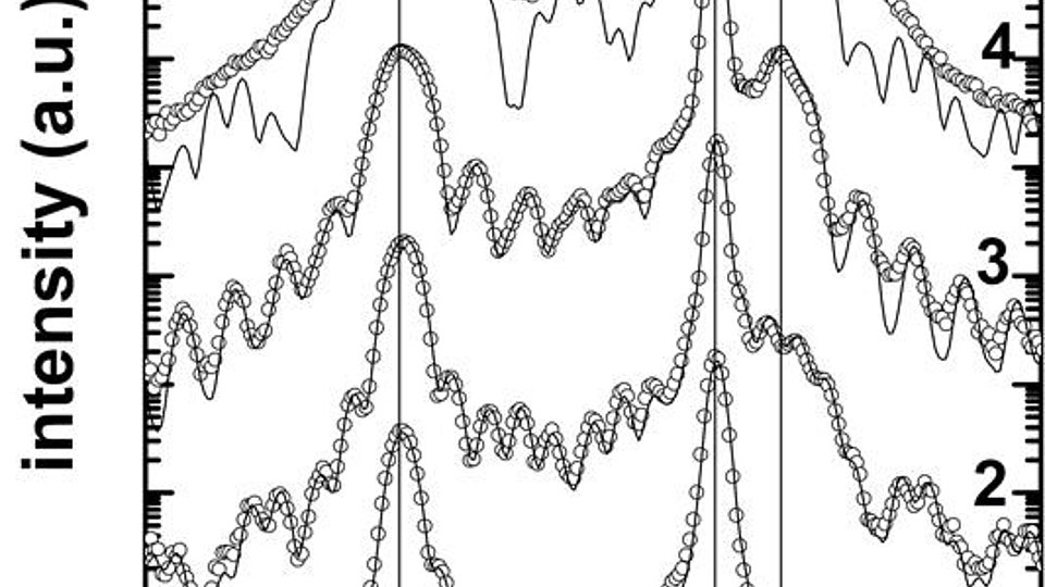
Fig. 1b: HRXRD measurements of 4 samples in (a) - sample 4 does not show any fringes -► deteriorated crystal quality.
Edge emitting semiconductor diode lasers designed for high output power are preferably realized in the GaAs/AlGaAs material system. By broadening the vertical intensity distribution across the cavity the facet load decreases, which allows for higher optical output power. This usually requires layer stacks with an overall thickness above 6 µm. Furthermore, bipolar cascade lasers ("nanostacks") are suited for very high power applications as well. These are formed by stacking several lasing stages monolithically, i.e. during epitaxial growth, with each stage, including the active region, embedded into waveguide and cladding layers. Inbetween the stages, tunnel junction diodes are located to form a low resistance electrical interconnection.
Although the room temperature lattice mismatch of ~0.14% between AlAs and GaAs appears rather small, overall thicknesses larger than 6 µm can lead to a convex wafer bow with a radius of curvature below 6 m. This can cause issues during wafer processing and is also known to trigger early device failure. Therefore, wafer bow and overall strain in such semiconductor diode lasers, primarily consisting of AlxGa1‑xAs waveguide and cladding layers, are to be minimized.
Our favored approach to achieve this is to replace part of the arsenic atoms in the AlxGa1‑xAs cladding layers with smaller phosphorus atoms. This decreases the lattice constant and lowers the compressive strain. AlxGa1‑xAs layers have a much lower compressive strain of ≤0.02% at usual growth temperatures between 700-800°C compared to room temperature. Thus, a typical phosphorus mole fraction of 1-4% will cause the growing AlxGa1‑xAsy P1-y layer to be under tensile strain. In order to prevent formation of dislocations or even cracks during growth the strain-dependent critical thickness must not be exceeded.
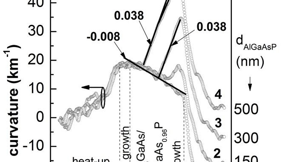
Such a growth process is ideally monitored and controlled by using in-situ curvature measurements. Fig. 1a shows curvature transients during growth of AlxGa1‑xAsy P1-y layers using metal-organic vapor phase epitaxy (MOVPE). The growth of a 500 nm thick Al0.85Ga0.15As0.96P0.04 layer already over-compensates the compressive room temperature strain of a 150 nm thick Al0.85Ga0.15As layer. However, as is shown in Fig. 1b the corresponding HRXRD measurement indicates a deteriorated crystal quality for that sample. In contrast, a 300 nm Al0.85Ga0.15As0.96P0.04 layer (3) leads to a rather small residual room temperature strain, but high crystal quality is maintained.
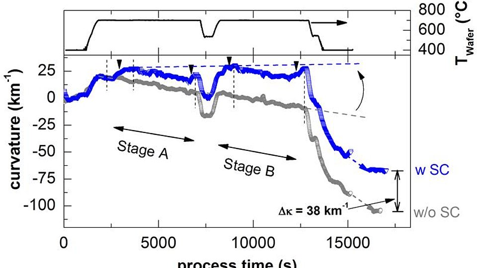
Consequently, instead of growing one thick layer of AlxGa1‑xAsy P1-y it is advisable to distribute several thinner AlxGa1‑xAsy P1-y layers across the vertical layer sequence. Such a distributed strain compensation scheme was applied to a 2-stage nanostack as shown in Fig. 2. Here, the four up to 350 nm thick Al0.85GaAs cladding layers were partly replaced by Al0.85Ga0.15As0.96P0.04 (arrows in Fig. 2). This results in a curvature reduction of 38 km-1.
In conclusion, in-situ curvature measurements are well suited for optimizing overall strain as well as the strain distribution across complex layer structures.
Publication:
A. Maaßdorf, U. Zeimer, M. Weyers, "MOVPE-grown AlxGa1-xAsyP1-y strain compensating layers on GaAs", J. Cryst. Growth 370, pp. 150-153 (2013).
FBH research: 21.05.2013


