Assessment of real wafer temperature of GaN/Saphir with new in-situ sensor
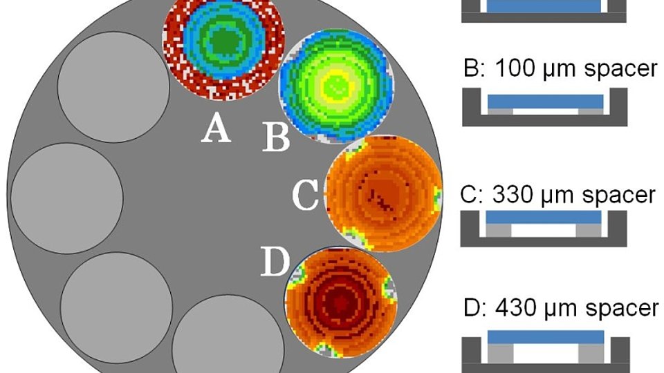
Fig. 1: PL wavelength of InGaN/GaN multi quantum wells on GaN/sapphire templates with spacers of different thickness and thus different temperature of the surface. The color code spans the wavelength range from 390 nm (violet) to 460 nm (dark red).
Growing GaN layers on sapphire substrate by metal organic vapor phase epitaxy leads to bowing of the wafers due to lattice mismatch and thermal expansion coefficent differences between substrate and layer. Larger wafers (for example 150 mm) that are increasingly used in production can bow during growth by several 100 µm depending on the layer design. Such bow also affects the temperature of the wafer that cannot be assessed by conventional pyrometry in the infrared as the material is transparent. Inhomogeneous wafer temperature leads to reduced yield since incorporation in InGaN-based LED and laser heterostructures and thus the emission wavelength is very sensitive to the temperature at the growth front.
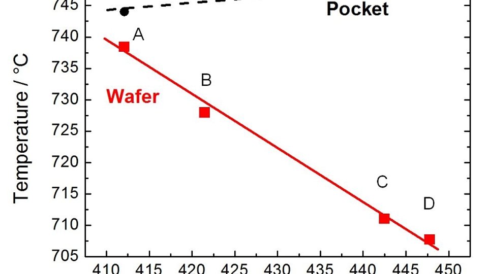
In cooperation with LayTec as manufacturer of in-situ sensors, FBH has tested a new temperature sensor (Pyro 400) that measures the surface temperature of InGaN by pyrometry at around 400 nm. InGaN/GaN quantum wells were grown on GaN templates on 100 mm diameter sapphire substrates monitoring the temperature of the wafer surface as well as that of the pocket holding the wafer. Thin sapphire spacers under the wafer were used to increase the temperature offset between wafer and pocket. The PL wavelength of the quantum wells depend on the spacer thickness and show a redshift by 40 nm for 430 nm spacer (Fig. 1). While the temperature of the pocket is only marginally affected by the spacers, the wafer temperature differs by about 40 K between a wafer directly lying in the pocket and the one with 430 µm distance. This shift of PL wavelength is correlated to the wafer temperature with 1.1 nm/K. Since the temperature difference between pocket and wafer surface is affected, for example, by the thickness grown on the susceptor, a precise knowledge of the wafer temperature is indispensable for an exact adjustment of the emission wavelength of the devices.
Publication
V. Hoffmann, A. Knauer, F. Brunner, S. Einfeldt, M. Weyers, G. Tränkle, K. Haberland, J.-T. Zettler, M. Kneissl "Uniformity of the wafer surface temperature during MOVPE growth of GaN-based laser diode structures on GaN and sapphire substrate", J. Cryst. Growth, vol. 315, no. 1, pp. 5-9 (2011).
FBH research: 19.06.2012

