Design, Fabrication, and Characterization of Miniaturized AuSn Flip-Chip Transitions up to 110 GHz
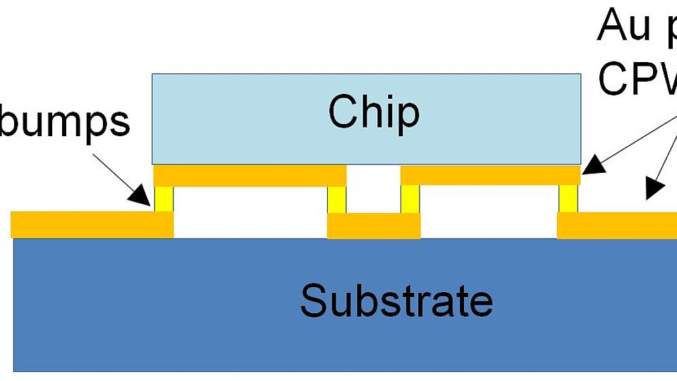
For high-frequency applications in the mm-wave through to the sub-THz spectrum, miniaturized flip-chip mounting (as schematically depicted in Fig. 1a) is a very attractive packaging solution. Compared with wire bonding attachment of semiconductor chips in hollow-core waveguide assemblies, flip-chip mounting offers wider bandwidth due to smaller parasitic inductances, better mechanical stability, and a smaller package size. Typical dimensions of waveguide strips and bump diameter scale to ~10 µm for the frequencies under consideration between 110 GHz and 350 GHz. These feature sizes can easily and accurately be produced using semiconductor fabrication methods. The resulting high-frequency transitions and assemblies can be well modeled thanks to the low fabrication tolerances.
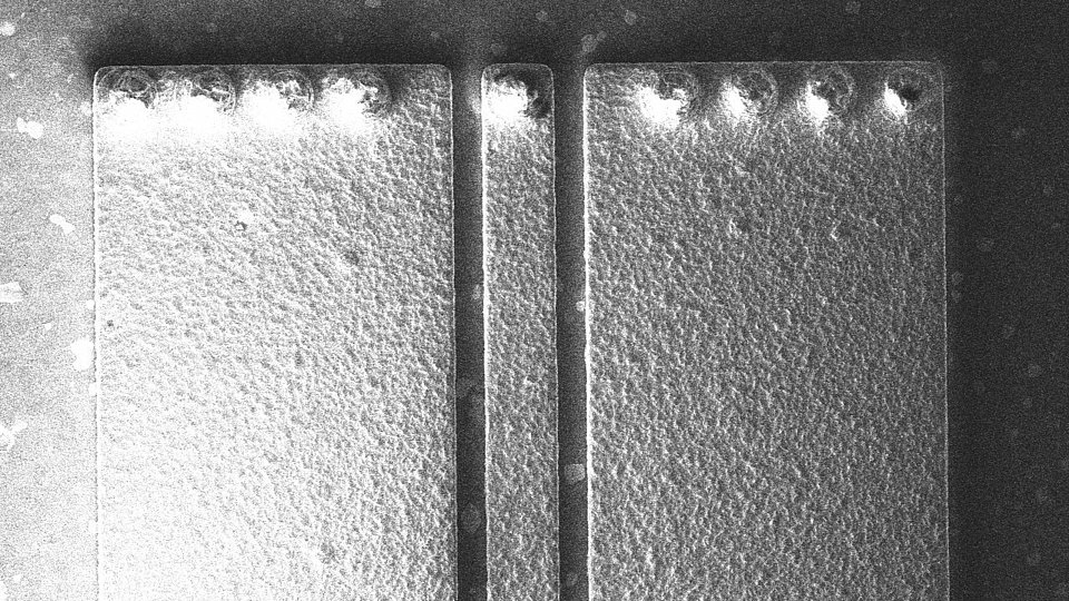
The technology to process small-size (< 10 µm bump diameter) AuSn bump flip-chip transitions has been developed. AuSn is selected as the bump material due to its proven bonding stability and reliability. Coplanar waveguide lines (CPW) were fabricated by Au electroplating on both quartz or aluminum nitride (AlN) chips and the AlN carrier substrate. The 6 µm thick multilayers of AuSn bumps, with 80% wt. Au and 20% wt. Sn summary composition, were evaporated on top of the CPW lines of the chip side. The AuSn bumps were structured in an i-line stepper-defined lift-off process (see Fig. 1b). Chip and substrate were bonded by means of an FC-150 commercial flip-chip bonder with lateral placement accuracy of better than 2 µm.
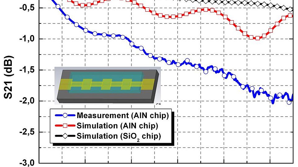
The measured small-signal transmission curves show a loss which is gradually increasing with frequency. Most of the losses can be attributed to line loss. By subtracting the line loss, we can extract the insertion loss of the actual flip-chip transition. At 110 GHz an insertion loss of -2 dB and a return loss of less than -15 dB were recorded for a device with a total of the eight transitions in series. The insertion loss is demonstrated in Fig. 2. The simulations shown here exclude the ohmic losses in the transmission line’s conductor metal. A thru-line of equal length as the device yielded approximately 1 dB loss. As a result, we can give an upper bound for the insertion loss of less than 0.5 dB per transition. The return loss and the ripple on the transmission can be suppressed by adjusting the CPW line dimensions: the design presented here was calculated for a SiO2 chip material, while the final tested device was fabricated using an AlN chip with different dielectric constant. The dielectric constant values of SiO2 and AlN are 3.8 and 8.9, respectively.
In summary, the feasibility to fabricate miniaturized AuSn bumps (< 10 μm) was demonstrated, enabling chip-to-chip assemblies of currently up to 110 GHz. RF characterization of the flip-chip interconnects up to 110 GHz revealed a low transition loss of less than 0.5 dB per transition. This result confirms that the AuSn flip-chip technology is a very suitable packaging solution for mm-wave applications. We have conducted further EM simulations of refined structures, suggesting the feasibility of micro-flip-chip transitions with 350 GHz bandwidth.
Publication:
S. Monayakul, C. Wang, O. Krüger, N. Weimann, "Design, Fabrication, and Characterization of Miniaturized AuSn Flip-Chip Transitions up to 110 GHz", Proc. WOCSDICE 2013.
FBH research: 24.06.2013


