Short-channel effect-free 100 nm Ka-band transistors
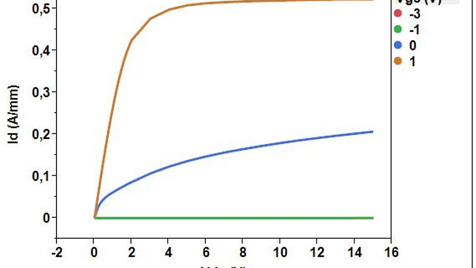
Fig. 1. Output characteristics of transistors with 100 nm gate length using standard (a), top) and new (b), bottom) epi-designs.
The Ka-band covers the frequencies from 26.5 to 40 GHz and enables high bandwidth communication systems. The frequency range is therefore well-suited for high data rate satellite communications, which is urgently needed. This opens up large market opportunities for microwave power amplifiers feeding these systems. GaN power amplifier MMICs seem to be good candidates due to their small dimensions, low weight, flexible system implementation, and low energy consumption – features being essential for space applications. The FBH has now developed the key gate technology for these devices and tested epitaxial layer structures adjusted to the short gates. An implementation of these modules in the existing GaN MMIC process is ongoing.
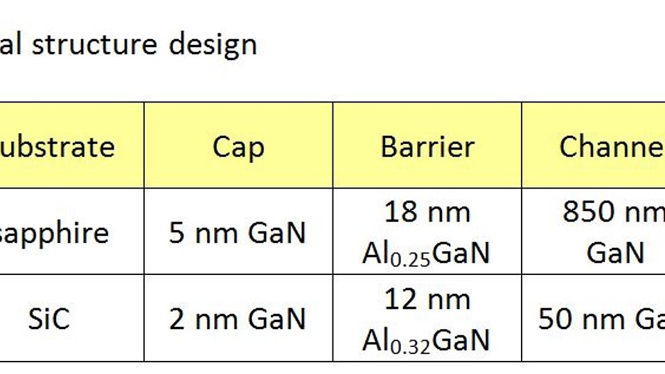
Fig. 1 compares two generations of 100 nm Ka-band transistors fabricated on different epitaxial structures according to table 1. The standard design representing an epitaxial layer sequence successfully applied in the 0.25 µm FBH MMIC process shows a distinct short channel effect, which means that the device cannot be pinched off anymore at a higher drain voltage. The comparably large gate to channel separation of 18 nm combined with the small gate length leads to a significantly compromised channel modulation at higher drain voltages. Thus, the so-called “punch-through effect” occurs (Fig. 1a). In order to overcome this issue, a modified epi-design has been developed. A much smaller gate-to-channel separation of only 12 nm increases the gate driving capability while an Al0.04Ga0.96N potential barrier to the buffer focusses the electrons to the channel region. A thinner AlGaN barrier is associated with a reduced electron concentration in the buffer. In order to compensate this, the Al concentration in the barrier has been increased from 25% to 32%.
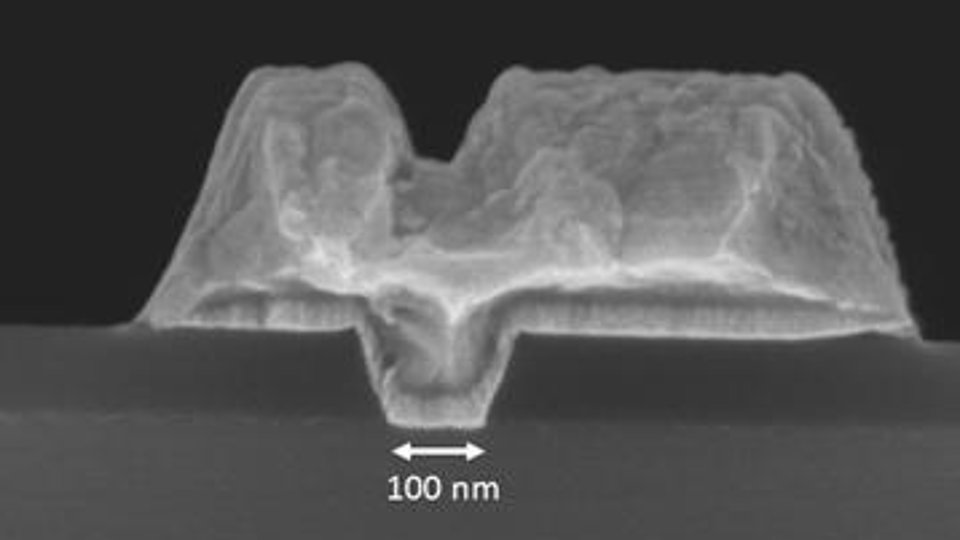
Fig. 1b shows that this structure is now very efficiently eliminating short channel effect. Preliminary electrical measurements of new transistors show a threshold voltage Vpo of -1 V, a transconductance gm of 380 mS/mm and a slightly lower Ids_max compared to previous devices. This means that the newly developed epi-structure fits well for short gate transistor fabrication. The combination of slanted sidewall gate fabrication technology (Fig. 1b) and new epitaxial structures allows for short-channel effect-free GaN HEMTs for Ka-Band applications.
Publication:
K.Y. Osipov, W. John, N. Kemf, S.A. Chevtchenko, P. Kurpas, M. Matalla, O. Krüger, J. Würfl: "Fabrication technology of GaN/AlGaN HEMT slanted sidewall gates using thermally reflowed ZEP resist and CHF3/SF6 plasma etching" Int. Conf. on Compound Semiconductor Manufacturing Technology (CS ManTech 2013), New Orleans, USA, May 13-16, paper 041 (2013).
FBH research: 13.11.2013


