UV laser scribing for die separation of GaN-based lasers
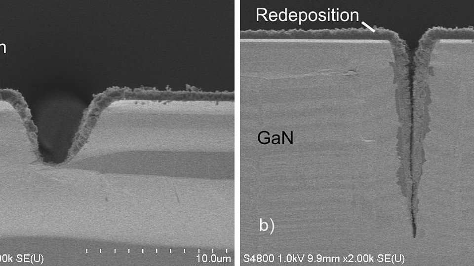
Fig. 2: Cross-sectional scanning electron micrographs of laser scribed trenches in GaN at a scribe speed of 100 mm/min and laser pulse energies of (a) 0.5 µJ and (b) 3.5 µJ yielding to depths of 5 µm and 33 µm, respectively.
High brightness ultraviolet (UV) laser diodes on the basis of AlInGaN epitaxial layers are currently fabricated on 2 inch GaN wafers. The laser resonator of these edge emitters is defined by the facets whose quality determines device performance. Die separation by breaking the wafer in pieces is one critical step for fabricating high-quality laser facets without terraces and other defects. Moreover, the group-III nitride layers and the GaN substrate crystallize in the hexagonal wurtzite structure that does not provide perpendicular crystal planes for easy cleaving cuboid-shaped laser chips. Laser-assisted techniques, such as laser cutting or scribing, provide versatile methods to address this issue.
At FBH nanosecond-pulsed laser radiation (pulse length < 30 ns) with a wavelength of 355 nm is successfully used to scribe the material followed by cleaving. At 355 nm GaN absorbs, decomposes and ablates which allows for efficient laser micromachining. Processing parameters, such as pulse energy, pulse repetition frequency (PRF), and scan velocity were optimized to avoid damage to the laser active region and obtain best device performance.
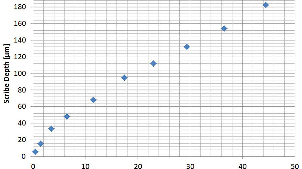
In contrast to conventional scribing by means of a diamond tip, laser scribing does not suffer from abrasion of the tool and the scribe depth can more widely be adjusted according to the needs of the breaking process. The last-mentioned point is illustrated in Fig. 1 that shows the scribe depth as a function of the laser pulse energy. Fig. 2 shows corresponding cross-sections of two laser cuts at different laser pulse energies. The scanning electron micrographs taking before subsequent cleaning still show redeposited material in the trench and near the machined area.
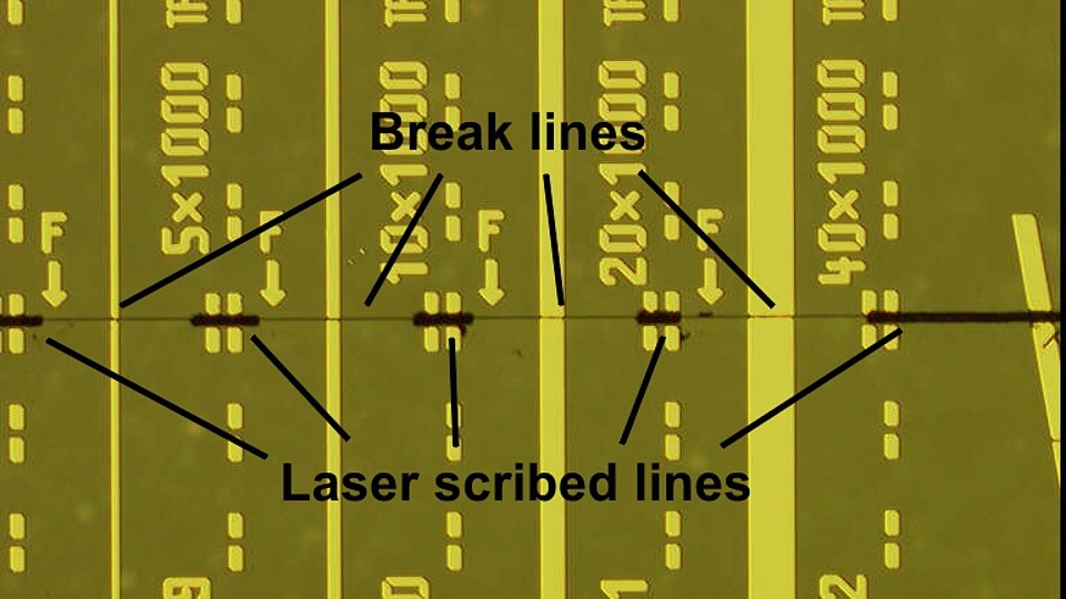
While diamond scribing works excellently for materials with cubic-like crystal structures such as GaAs and silicon, it suffers from low yield when scribing and cleaving rectangular chips of hexagonal GaN-based crystals. A laser scribe line can be placed very flexibly thereby forcing the cleave plane into the desired direction and increasing significantly the yield of the laser dies. As an example Fig. 3 shows a dashed scribe line that guides the breaking along the boundary line of the devices, i.e. the line on the wafer’s front is interrupted near the laser ridge of the diode laser thereby avoiding any damage to the laser facets. To minimize the number of particles on the surfaces caused by redeposited material during laser processing, a water-washable protective coating is applied to the front of the wafer just prior to laser scribing. After processing the coating is washed with room temperature de-ionized water thereby removing particle contamination generated from material ablation.
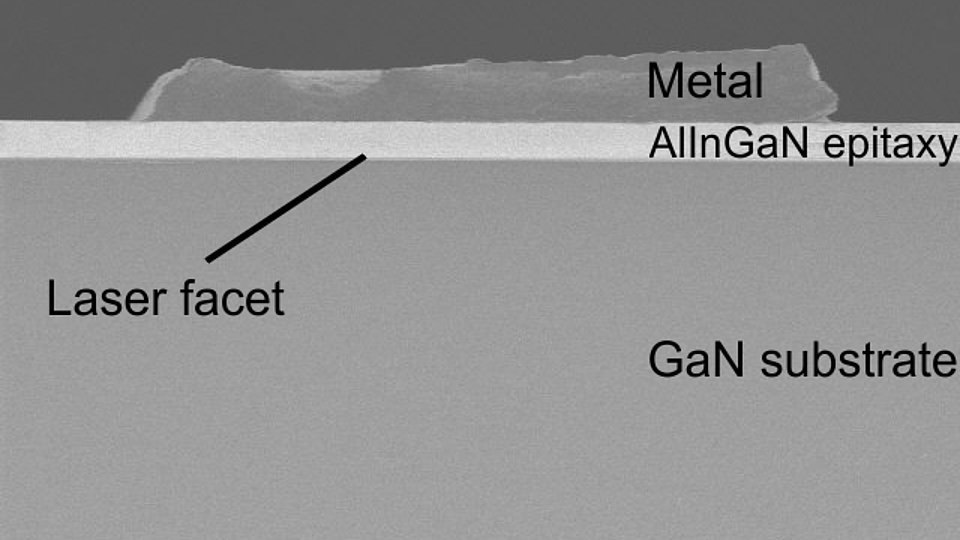
Fig. 4 shows a detailed view of a laser facet after laser-assisted die separation. The facet is free of particle contamination and terraces. When operating the laser diodes there is no indication of degradation of laser performance compared to devices separated by conventional diamond scribing and breaking. However, the laser-assisted process provides more process stability in terms of die yield and the overall processing time is about half of the diamond-based process flow. Further investigations on potential process-induced changes of optical performance and material properties are currently ongoing.
FBH research: 28.07.2014


