Development of slanted gates for AlGaN/GaN HEMTs
Two new process sequences for the formation of slanted gates have been developed at the FBH – the advanced gate modules are ready for integration into GaN-based HEMT and MMIC technology. They allow the formation of slanted gates with dimensions down to 50 nm, as required for many sophisticated applications including radar and communication systems. The new processes will be used for highly efficient high-power transistors based on AlGaN/GaN hetero-junction field effect transistors (HFETs) offering novel solutions for high-end applications.
Gate fabrication is a crucial part in transistor manufacturing due to its strong influence on device performance and reliability. Currently, the most commonly used technology for GaN-based HEMTs and MMICs is the so-called “embedded gate” process, where the gate metal is deposited into a vertical trench opening that is etched in a dielectric passivation layer usually consisting of silicon nitride. The semiconductor surface properties at the bottom of the trench opening along with the semiconductor/metal interface quality determine the electrical characteristics and reliability of the transistors. Trench etching of the dielectric layer needs to be carefully controlled to avoid detrimental effects on the semiconductor surface. Moreover, this etching should provide a trench geometry that allows for conformal metal coverage without void formation. A trapezoidal profile of the gate trench will also reduce the electric field predominantly at the drain side edge and thus improve the device reliability and reduce dispersion effects. The following approaches towards slanted gates have been successfully developed; their respective advantages and disadvantages are currently further investigated:
Resist reflow and dry etch approach
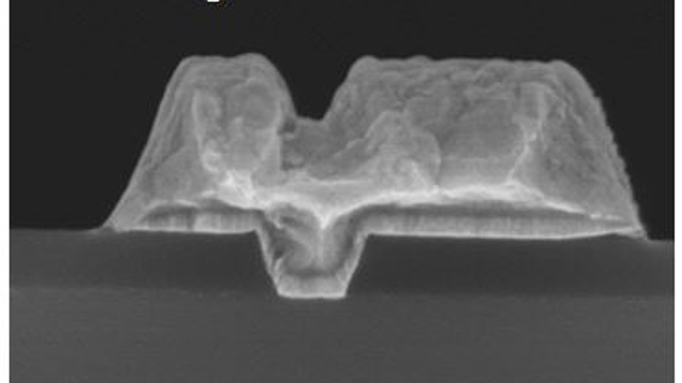
This method aims at reaching smallest gate dimensions in combination with the slant in one etch step only. It bases on reflow of ZEP 520A e-beam resist followed by plasma etching. The thermal reflow of the resist results in a profile rounding and in an increased robustness during plasma etching. Temperature and duration of the reflow process determine the shrinking of the feature size and the slope of the sidewall in the resist opening. During plasma etching the shape of the resist will be transferred into the nitride. The sidewall angle can be reproducibly set between 55 and 75 degrees. Gate dimensions down to 50 nm have been realized using a highly anisotropic dry etch process. Fig. 1 shows SEM images of various Ir/Au gates fabricated on test wafers. Down to 50 nm long gates the trench sidewalls provide conformal trench coverage. The diode characteristics of 250 nm gate transistors indicate that the new process provides excellent Schottky contacts with leakage current levels far below 1 nA/mm and a barrier height of 1.1 eV, which is characteristic for Ir/GaN Schottky contacts. DC output characteristics and S-parameter measurements of such transistors processed on sapphire substrates are comparable to standard transistors having embedded gates with vertical sidewalls. The drain current characteristics exhibit excellent uniformity over the 3 inch wafer indicating high process conformity.
Combined dry-wet etch approach
This process relates plasma and wet chemical etching. After lithographically defining the trench, an anisotropic plasma etch is used to form a shallow trench in the upper part of the nitride layer first. Then, after resist stripping, the nitride is thinned and removed from the bottom of the trench by means of an isotropic wet chemical etch. The resulting slope of the slant depends on the remaining silicon nitride thickness after the initial shallow trench etching. This process sequence avoids any plasma damage of the semiconductor interface. Cross section of a 280 nm gate (not shown) proved slant and conformal metal coverage; the measured output characteristics of such a device are typical for that gate length.
Publications
K.Y. Osipov, W. John, N. Kemf, S.A. Chevtchenko, P. Kurpas, M. Matalla, O. Krüger, and J. Würfl: "Fabrication technology of GaN/AlGaN HEMT slanted sidewall gates using thermally reflowed ZEP resist and CHF3/SF6 plasma etching" Int. Conf. on Compound Semiconductor Manufacturing Technology (CS ManTech 2013), New Orleans, USA, May 13-16, paper 041 (2013).
A. Thies, N. Kemf, S.A. Chevtchenko, and O. Krüger: "Formation of Slanted Gates for GaN-Based HEMTs by Combined Plasma and Wet Chemical Etching of Silicon Nitride" Int. Conf. on Compound Semiconductor Manufacturing Technology (CS ManTech 2013), New Orleans, USA, May 13-16, paper 112 (2013).
FBH research: 06.11.2013
