Increased emission power of 380 nm UV-LEDs
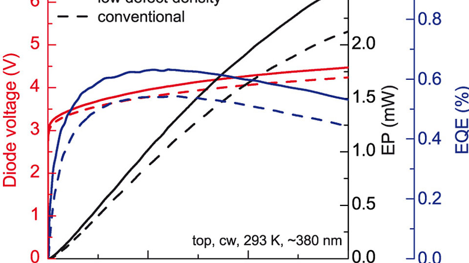
Fig. 1: PUI characteristics of a top-emitting 380 nm UV-LED structure with broad (solid line) or conventional n-AlGaN blocking layer (segmented line) underneath the active region.
The FBH is developing top-emitting UV-LEDs for sensor applications in cooperation with TU Berlin and the company Jenoptik. The work is performed within the regional growth core Berlin WideBaSe and focuses on the development of efficient LEDs with emission wavelengths between 360 and 380 nm. It was possible to increase the efficiency of the epitaxial structure by applying a couple of growth and heterostructure adjustments.
Since high emission power at low diode current densities are required for the desired application, a single quantum well structure was used as active region instead of a 5x InGaN/AlInGaN MQW. In addition, the AlGaN blocking layers underneath and on top of the active region that prevent the overflow of minority charge carriers were adjusted in order to improve the majority carrier injection. By increasing the thickness of the AlGaN layer and decreasing the Al mole fraction, the electron injection into the active region is improved as a consequence of the modified band structure. Fig. 1 shows the characteristics of processed top-emitting LEDs with a conventional and a wide n-AlGaN blocking layer underneath the active region.
Furthermore, GaN-based devices on sapphire substrate suffer from the high number of dislocations threading from the GaN/substrate interface to the active region. By applying a defect reducing GaN buffer growth technique, the threading dislocation density in the active region could be reduced from 109 cm-2 to 3x108 cm-2. Thus, the recombination efficiency of the quantum wells could be increased. Fig. 2 shows the characteristics of identical LED heterostructures on a conventional GaN/sapphire template compared to a template with reduced defect density. By combining the optimizations it was possible to increase the external quantum efficiency of an LED structure emitting at 380 nm by more than a factor of two. In a next step, it is planned to shift the emission wavelength of the optimized heterostructure toward 360 nm, which is required for sensor applications.
Publications
A. Knauer, H. Wenzel, T. Kolbe, S. Einfeldt, M. Weyers, M. Kneissl, G. Tränkle, "Effect of the barrier composition on the polarization fields in near UV InGaN light emitting diodes", Appl. Phys. Lett., vol. 92, no. 191912 (2008).
A. Knauer, T. Kolbe, S. Einfeldt, M. Weyers, M. Kneissl, and T. Zettler, "Optimization of InGaN/(In,Al,Ga)N based near UV-LEDs by MQW strain balancing with in-situ wafer bow sensor", phys. stat. sol. (a), vol. 206, no. 2, pp. 211-214 (2009).
T. Kolbe, A. Knauer, H. Wenzel, S. Einfeldt, V. Kueller, P. Vogt, M. Weyers, and M. Kneissl, "Emission characteristics of InGaN multi quantum well light emitting diodes with differently strained InAlGaN barriers", phys. stat. sol. (c), vol. 6, no. S2, pp. S889-S892 (2009).
T. Kolbe, T. Sembdner, A. Knauer, V. Kueller, H. Rodriguez, S. Einfeldt, P. Vogt, M. Weyers, and M. Kneissl, "Carrier injection in InAlGaN single and multi-quantum-well ultraviolet light emitting diodes", phys. stat. sol. (c), vol. 7, no. 7-8, pp. 2196-2198 (2010).
T. Kolbe, T. Sembdner, A. Knauer, V. Kueller, H. Rodriguez, S. Einfeldt, P. Vogt, M. Weyers, and M. Kneissl, "(In)AlGaN deep ultraviolet light emitting diodes with optimized quantum well width", phys. stat. sol. (a), vol. 207, no. 9, pp. 2198-2200 (2010).
FBH research: 23.05.2012

