Atomic Layer Deposition – a powerful tool for atomic-scale processing
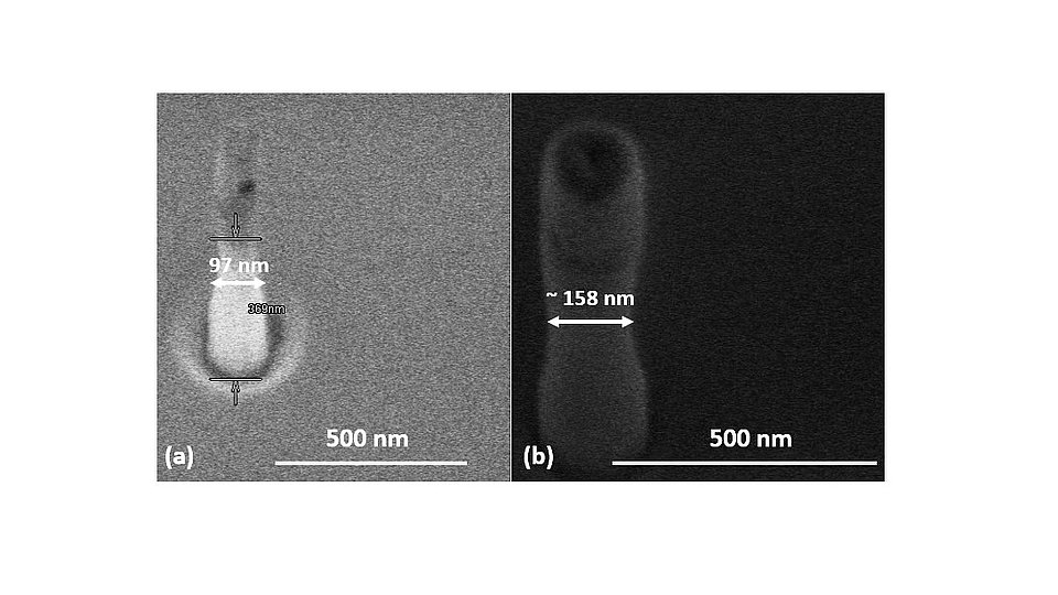
Fig. 1: Diamond nanopillar (a) before deposition and (b) after ≈30 nm ALD Al2O3 deposition increasing the diameter of the nanopillar conformally.
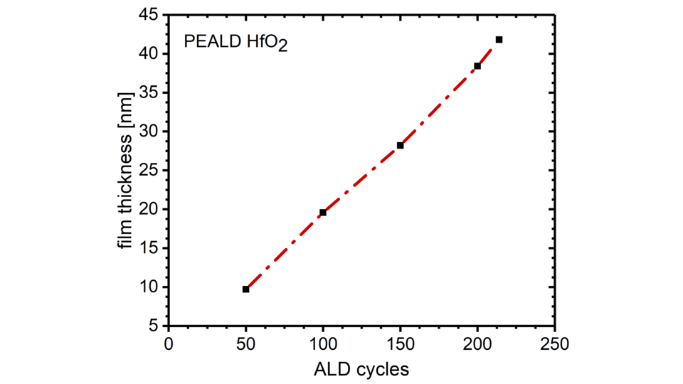
Fig. 2: Linear growth of PEALD HfO2 layers as a function of number of ALD cycles ensuring precise thickness control.
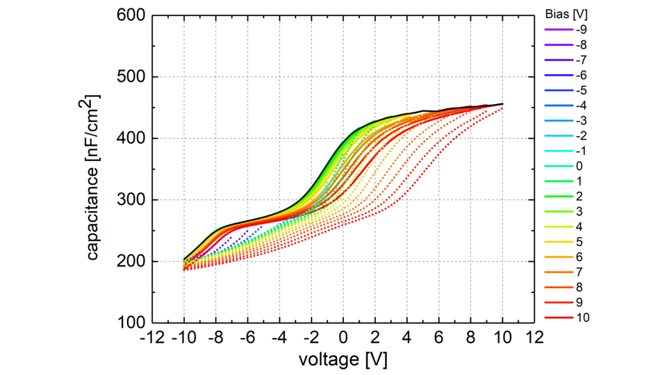
Fig. 3: CV-sweeps of MIS capacitor with PEALD HfO2 as the gate dielectric material, forward (solid) and reverse (dotted).
Due to the continuous shrinking of device sizes and the rising demand for 3D integration and complex substrates, advanced coating technologies have become essential. Atomic Layer Deposition (ALD) has emerged as a promising method to precisely develop high-quality nanolayers of various materials. This chemical coating technology relies on sequential and self-limiting reactions of gaseous reactants with the available functional groups on the substrate sites, allowing for atomic-scale control of thin film deposition. To grow nano- or Angstrom-scale layers, carefully chosen precursors are alternatively dosed on the substrate, separated by purge steps for removing excess reactants and reaction by-products in a cyclic manner. This surface-controlled nature of the ALD processes ensures high uniformity and superior 3D conformality on any arbitrary substrate geometries, as demonstrated in Fig. 1 for diamond nanopillars fabricated for quantum photonic investigations.
At FBH, we have developed ALD processes for two technologically relevant oxides: Al2O3 and HfO2. Beyond the conventional thermal ALD process, we utilize Plasma Enhanced ALD (PEALD) to grow dielectric layers at a lower temperature, such as 100° C, making it feasible for temperature sensitive substrates. PEALD offers greater flexibility in terms of process development, and the remote plasma configuration of our tool ensures no substrate damage due to plasma exposure.
We have successfully grown Al2O3 layers using Trimethyl aluminum (TMA) and H2O by thermal ALD, and O2 plasma as the oxidizing agent in the PEALD variant. This resulted in a growth of about 1.2 Å per cycle, a refractive index of approximately 1.65, and thickness non-uniformity within 1-2 % on a 100 mm wafer scale. The produced Al2O3 layers are amorphous, smooth, and stoichiometric; transitioning to polycrystalline upon annealing above 600° C.
For the development of PEALD HfO2 layers, we employed Tetrakis(dimethylamido)hafnium (TDMAH) and O2 plasma as precursors. Fig. 2 depicts linear growth of PEALD HfO2 layers as a function of the number of ALD cycles, indicating precise thickness control. We achieved a growth of about 1.9 Å per cycle, a refractive index of approximately 2.02 and non-uniformity less than 2 % on a 100 mm wafer scale. HfO2 layers remain amorphous up to about 100 nm at a 250° C growth temperature, with thicker films showing crystalline peaks corresponding to the monoclinic phase of HfO2. Further investigations into the evolution of the structural properties of HfO2 layers as a function of annealing temperature are ongoing.
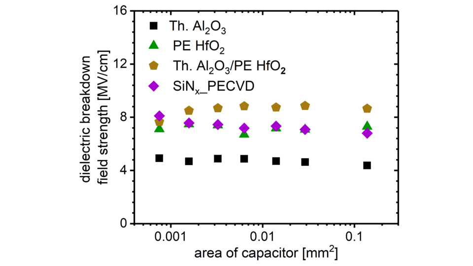
Our optimized process parameters have enabled films with a high refractive index, high density, good stoichiometry, low roughness, and minimal impurities, which are crucial for device applications. Such PEALD HfO2 layers are implemented as gate dielectrics in GaN-based MIS capacitors. Fig. 3 illustrates the CV-sweeps measurements for the HfO2-based MIS capacitors in forward and reverse bias. Comparative studies using MIM devices show that HfO2 films have a reasonably high breakdown field strength of about 8 MV/cm (see Fig. 4). Following this, we have also fabricated Al2O3/HfO2 nanolaminates to tailor a multitude of functionalities, ranging from refractive index, bandgap, and dielectric constant to breakdown strength. Our recent progress demonstrates a potential route to develop atomically controlled oxides, such as Al2O3, HfO2, and their nanolaminates with varying individual thicknesses and compositions. We are now tackling new challenges in terms of ALD process development for other oxides and nitrides and their novel applications in device technologies.
These activities were funded by the ECSEL Joint Undertaking (JU) under grant agreement No. 101007229. The JU receives support from the European Union’s Horizon 2020 research and innovation program and Germany, France, Belgium, Austria, Sweden, Spain, Italy. Funding from the European Research Council (ERC, Starting Grant project QUREP, Grant No. 851810), the German Federal Ministry of Education and Research (BMBF, project DiNOQuant, Grant No. 13N14921; project QPIS, Grant No. 16KISQ032K; project QPIC-1, Grant No. 13N15858; and project QR.X, Grant No. KIS6QK4001), and the Einstein Foundation Berlin (Einstein Research Unit on Quantum Devices) are acknowledged.
Publication
P. Paul, E. Brusaterra, I. Ostermay, E. Bahat Treidel, F. Brunner, K. Udas, O. Hilt, O. Krüger, ”Plasma Enhanced Atomic Layer Deposition of Hafnium Oxide (HfO2) Thin Films for MIM and GaN-MIS Devices”, AVS ALD/ALE 2024, Helsinki, Finland.


