Exploration of high-temperature PECVD SiNx for strain engineering of GaN-HEMTs
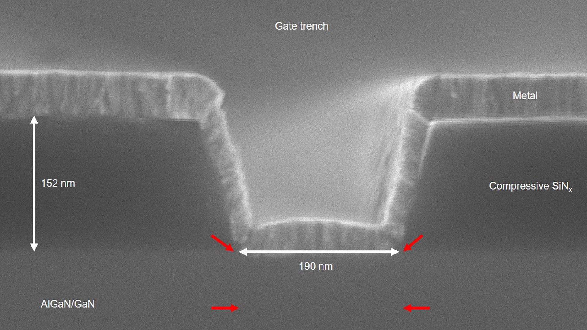
Fig. 1: SEM cross section image of an AlGaN/GaN- SiNx stack with a gate trench etched through the compressively stressed SiNx and a metal layer on top. The red arrows mark the stress direction within the SiNx and the strain direction within the AlGaN/GaN layers.

Fig. 2: Dependence of plasma excitation frequency (HF: High frequency at 13.56 MHz; LF: Low frequency at 100 kHz) and deposition temperature on mechanical stress in SiNx.

Fig. 3: Threshold voltage Vth of AlGaN/GaN HEMTs with differently stressed SiNx passivation layers. The mean value for HEMT with stress-free SiNx is -1.89 V, for the transistor with compressive SiNx as passivation layer it is -0.53 V.
In recent years, AlGaN/GaN high electron mobility transistors (HEMTs) have become an essential part of high-frequency and power electronics due to their high breakdown voltage, electron mobility, and saturation velocity. Unlike silicon transistors, GaN transistors are normally-on, meaning a control over the threshold voltage Vth is needed for future GaN applications, such as in 5G mobile communication to improve device performance and efficiency. Therefore, efforts are being made to develop tailored AlGaN/GaN transistors.
Our approach aims to influence the density of the two-dimensional electron gas (2DEG) in AlGaN/GaN structures by mechanical stress. By depositing a strained passivation layer onto the semiconductor stack, external mechanical stress is transferred to the underlying regions, as illustrated in Fig. 1. Compressive stress reduces 2DEG density, causing the threshold voltage Vth of the transistors to shift towards positive values, tensile stress does the opposite.
At FBH, we use Plasma Enhanced Chemical Vapor Deposition (PECVD) to deposit compressive silicon nitride (SiNx) passivation films. Our deposition tool provides a versatile process environment with temperatures up to 800°C and offers both high-frequency (HF) and low-frequency (LF) plasma excitation options. Fig. 2 illustrates the dependence of these deposition parameters on the stress in SiNx. We observe that combining HF and LF excitation generates compressive stress in the SiNx films. Additionally, increasing the deposition temperature from 300°C to 600°C enhances compressive stress from - 1000 MPa to - 1850 MPa.
The layers deposited at 300°C lose up to 50% of their stress throughout thermal treatment during subsequent process steps due to gradual relaxation. In contrast, SiNx deposited at 600°C has the advantage of being thermally stable. The high-temperature deposition results in a much denser film, making it less prone to stress relaxation. This stability is particularly important for reproducible stress values. Further, it is possible to generate a pulsed LF in combination with a HF excitation to tailor the stress in a range from 600 MPa to – 1800 MPa.
We have successfully implemented high compressive stressed SiNx passivation layers deposited at 600°C into our standard AlGaN/GaN HEMT process on 100-mm-wafers, resulting in changes of Vth as shown in Fig. 3. Our method has achieved a positive shift of up to 1.4 V, demonstrating its effectiveness. We are now working on further optimizations of both the SiNx layers and the overall process in order to be able to tailor the threshold voltage up to 0 V and beyond.