Packaging of UV LED chips to meet application demands
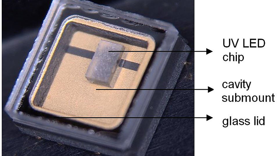
Fig. 2: UV-B LED chip after flip-chip soldering in a cavity submount for SMD mounting with a glass lid on the top
UV LEDs are highly attractive for various applications. They can be used, for example, for water purification, medical diagnostics, curing of adhesives and plant growth lighting. Besides improving the optical power and efficiency of the chip itself, packaging of UV LED chips is just as important. This is especially true with respect to thermal conductivity, hermeticity, low production costs, and industrial-suited processes.
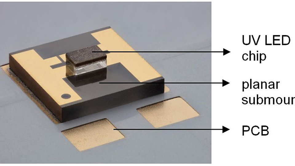
At FBH, UV LED chips are usually soldered onto planar AlN submounts (3.5 mm x 3.5 mm) with deposited ~4 µm thick Au80Sn20 solder, as can be seen in Fig. 1. This package provides good heat dissipation and is suited for SMD mounting. However encapsulation, hermetic sealing and simultaneous soldering of chips (as the chip needs to be pressed down during soldering) are hard to realize in this way.
More advanced packaging approaches make use of cavity AlN submounts of the same foot-print and have recently been developed at FBH. Since there is usually no solder deposited in the cavity, Au80Sn20 solder paste had to be dis-pensed. Afterwards, the UV LED chip was flipped, placed and soldered with a die bonder (Fig. 2). The solder thickness after the reflow process was around 15 µm. Shear tests and electro-optical tests confirmed that the mounting process was successful. UV-B LED chips mounted on planar and cavity submounts showed a similar performance when comparing the L-I-V characteristics (Fig. 3).
For applications where UV LEDs have to be operated in a harsh environment, e.g. under high humidity, the cavity submounts allow for simple chip protection. The chip is sealed by soldering a planar glass lid using an Au80Sn20 solder ring on top of the cavity submount (Fig. 2). Beyond that, these cavity submounts have the advantage that they reduce packaging costs because chips can be simultaneously soldered on a submount array.
In summary, the use of a cavity package for UV LED chips has been established at FBH in addition to the standard planar submount. This advanced package is comparable with the planar submount in terms of optical output power and efficiency. In addition, hermetic sealing of the UV LED chips was successfully demonstrated.


