Stabilization of AlN/sapphire templates during high-temperature annealing
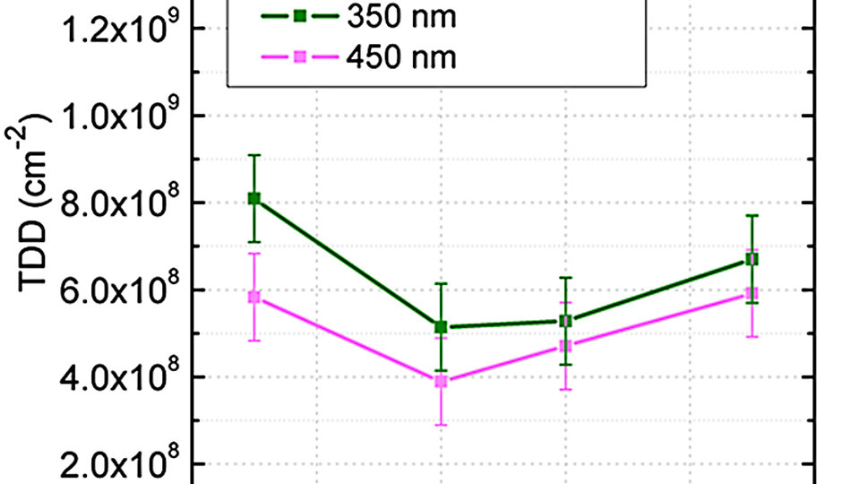
Fig. 1: Threading dislocation density (TDD) vs. annealing temperature for 350 nm and 450 nm sputtered AlN/sapphire templates after high-temperature annealing
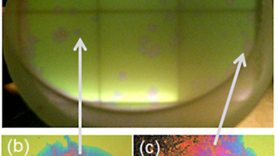
Fig. 2: Whole 2-inch wafer after annealing at T ≥ 1680 °C (a). Volcano-like defects (b) are distributed across the wafer while the wafer edge (c) also shows degraded material, which is attributed to polycrystalline AlON
To obtain high-performance AlGaN-based optoelectronic devices, AlN starting layers with low threading dislocation densities (TDD) below 109 cm-2 are required. Usually AlN/sapphire templates grown by metalorganic vapor phase epitaxy (MOVPE) are used. Unfortunately, the high lattice mismatch between sapphire and AlN initially leads to very high TDDs. To reduce this mismatch, down to 109 cm-2 thick AlN layers (> 3 µm) are commonly grown to benefit from dislocation annihilation with increasing AlN layer thickness. Therefore, complex growth processes are needed to avoid layer cracking. A new and promising approach to realize AlN layers with low TDDs of 4 x 108 cm-2 is high temperature annealing (HTA) of thin (< 1 µm) sputtered AlN/sapphire layers at elevated temperatures about 1700 °C, causing dislocation movement and annihilation in the AlN layer. This comparably inexpensive technique offers further advantages, such as a reduced wafer bow due to the thinner AlN layers, which makes processing of devices using optical lithography much easier. First promising results of AlGaN-based UVC LEDs on top of such templates have recently been demonstrated within the Joint Lab GaN Optoelectronics together with TU Berlin [1].
As starting substrate for the HTA process, we used reactively sputtered 350 nm and 450 nm thick AlN on 2-inch c-plane sapphire substrates leading to initial TDDs of 3 x 1010 cm-2. We studied the annealing process of these samples using a sintering oven at temperatures between 1650 °C and 1730 °C for 3 hours in nitrogen atmosphere at 1000 mbar. To stabilize the AlN surface, always two samples were placed face-to-face: AlN layer on AlN layer. The obtained TDDs after annealing are shown in Fig. 1 as a function of annealing temperature and layer thickness. For T = 1680 °C and 450 nm layer thickness the most effective TDD reduction by almost two orders of magnitude (TDD = 4 x 108 cm-2) was achieved.
For T 1680 °C the AlN layer at the wafer edges unfortunately started to degenerate, and macroscopic defects in the shape of volcanos appeared scattered across the wafers (Fig. 2). Both effects can be attributed to the formation of polycrystalline AlON spreading from the AlN/sapphire interface. This can be explained by a chemical solid phase reaction between AlN and sapphire to AlON in the relevant temperature range. Additionally, even in regions without polycrystalline AlON at the AlN/sapphire interface, the occurrence of epitaxial AlON (111) on the AlN (0001) surface after annealing could be observed (Fig. 3) by using high-resolution scanning transmission electron microscopy (HR-STEM). Interestingly, for HTA at 1700 °C, this formation only took place for the 350 nm thick AlN layer, but not for the thicker layer. The AlON on the surface hinders MOVPE overgrowth and must be avoided to produce templates usable for device fabrication. Excessive oxygen has to reach the surface resulting in AlON formation. This oxygen is most likely supplied by diffusion from the sapphire substrate to the layer surface along the initially high number of threading dislocations. However, this process is not yet fully understood. Further investigations have to be carried out to ensure preservation of the AlN surface during HTA for subsequent MOVPE growth.
In summary, a new technique of manufacturing AlN/sapphire templates with encouraging first results has been presented. However, stabilization problems leading to polycrystalline AlON at the interface and formation of epitaxial AlON on the AlN surface need to be overcome. Here, optimal combinations of layer thickness and annealing time are being studied aiming to develop a stable process.
Publication
N. Susilo, S. Hagedorn, D. Jaeger, H. Miyake, U. Zeimer, C. Reich, B. Neuschulz, L. Sulmoni, M. Guttmann, F. Mehnke, C. Kuhn, T. Wernicke, M. Weyers, and M. Kneissl, "AlGaN-based deep UV LEDs grown on sputtered and high temperature annealed AlN/ sapphire", Appl. Phys. Lett., vol. 112, no. 04, pp. 041110 (2018).


