Enhancing Modeling Accuracy - Simulating Drain Lag of GaN HEMTs with ASM-HEMT
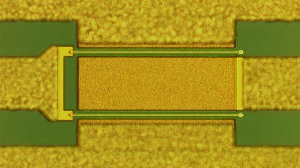
Nowadays, GaN HEMTs (Fig. 1) receive great recognition in microwave applications when high power, low noise, and/or operation under tough conditions are demanded. The GaN industry, with the purpose of supporting applications’ designs, provides large-signal compact models that are capable to describe one major issue, the trapping effects. A well-developed compact model is characterized by high accuracy, good convergence properties, usefulness in circuit design, and preferably with physical insight. With such capabilities, we can bridge the gap between experiment and modeling of semiconductor devices. At FBH, we use the ASM-HEMT physics-based compact model within our joint activities with BTU Cottbus-Senftenberg. We have enhanced this model with a drain-lag implementation that best describes our GaN HEMTs [1], establishing a connection between design and technology.
Due to the great progress regarding semiconductor surface passivation and treatment, gate-lag effects have been significantly reduced. However, drain lag can still hamper device performance, resulting in inconsistent simulations if omitted. Thus, we developed a drain-lag model for ASM-HEMT, enhancing the modeling accuracy as well as the physical insight of the original model’s drain-lag description. Our approach relies on scaling three model parameters according to the quiescent bias, with a focus on trap-affected physical properties, good numerical convergence, and efficient extraction procedure as well. With our implementation, ASM-HEMT is capable to cover changes on device behavior created by drain-lag effects without compromising modeling performance in circuit design.
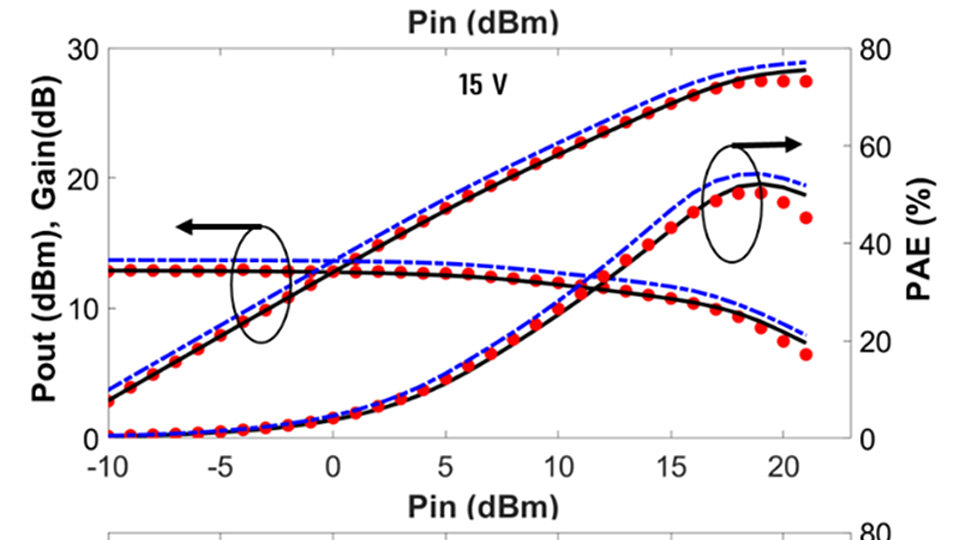
Fig. 2 presents measured and simulated output power, power-added efficiency and gain at 8 GHz in a bias region related to class-AB amplifiers. The load was adjusted for providing maximum output power. In this figure, simulation results from ASM-HEMT without any trap model are compared with ASM-HEMT driven by the drain-lag model we developed. The model without considering any trapping effects shows its inability to predict real device behavior for the whole range of biases and input power. On the other hand, the results of the model with the drain-lag implementation are almost identical to the measurements for all three applied voltages. The consideration of drain-lag effects appears to be a determinative factor for accurate large-signal modeling of GaN-HEMTs.
Publication
[1] P. Beleniotis, F. Schnieder, M. Rudolph, ‘‘Simulating Drain Lag of GaN HEMTs with physics-based ASM model’’, to appear in European Microwave Integrated Circuits Conference 2020, January 2021.

