Fabrication of customized beam splitters on diamond for ultrashort pulses in the mid-infrared
Fig. 1: Detail of the beam splitter imaged by optical microscopy showing the grating pattern with the golden shining metallic stripes
Beam splitting optics are required for most time-resolved measurements. They are commercially available for the visible and near-infrared spectral ranges, but their availability drops for longer wavelengths to nearly zero. Researchers from the Max Born Institute for Nonlinear Optics and Short Pulse Spectroscopy (MBI) and the Institute of Physics at Humboldt University Berlin designed a beam splitter for ultrashort pulses in the mid-infrared and terahertz spectral range. They identified diamond as well-suited medium for the intended application. At FBH, the beam splitters were fabricated on diamond plates by formation of metal gratings with 3 micron period and a coverage factor of about 0.65. Characterization of the beam splitters at MBI revealed that they keep the temporal pulse shape unchanged and they exhibit a nearly perfect phase shift and a reasonably constant splitting ratio [1].
The FBH manufactured the beam splitters on diamond substrates synthesized by chemical vapor deposition (CVD). The substrates are double-sided polished, 0.7 mm thick, and of elliptic shape having a long axis of 50 mm and a short axis of 20 mm. Due to the noncircular shape along with the target feature size of 1 micron, conventional photolithographic patterning using contact and stepper exposure tools could not be applied. The excellent surface flatness of the substrates and the application of a special chuck, however, allowed for use of electron beam lithography.
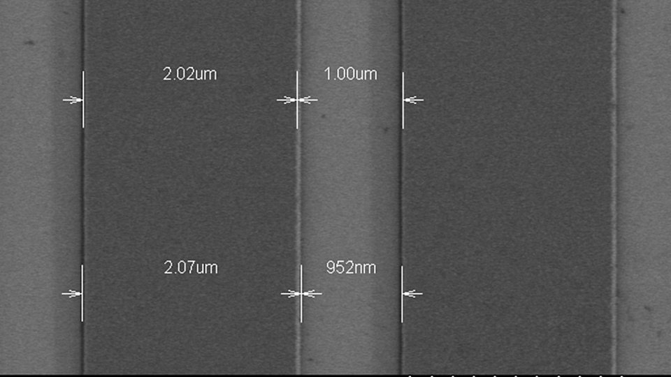
The metal gratings were generated by metal lift-off technique. For this purpose, a bi-layer system of poly(methyl methacrylate) (PMMA) resists with different molecular weights (AR-P 639.10 and AR-P 679.04, ALLRESIST) was spun on the samples. The conductive polymer ESPACER (Showa Denko K.K.) was applied on top to prevent negative charge build-up during electron beam exposure. The samples were exposed using an electron beam writer Vistec SB251. Due to the different sensitivity of the two PMMA resists, an undercut profile was obtained after development. Titanium and gold layers with 15 nm and 105 nm thicknesses, respectively, were deposited by electron-beam evaporation and finally patterned by gentle metal lift-off (Fig. 1). As depicted in Fig. 2, the regular pattern generated consisted of 2 micron wide gold stripes separated by 1 micron wide openings and covered the whole surface area except for an about 2 mm wide edge exclusion.
In summary, for flexible pattern adaptation and prototyping electron beam lithography is ideally suited on the micron and sub-micron scale, which provides a technology to customize such beam splitters by tailoring the period and coverage of the metal stripes to the wavelengths and splitting ratios needed.
Reference
C. Somma, K. Reimann, M. Woerner, T. Kiel, K. Busch, A. Braun, M. Matalla, K. Ickert, O. Krüger, "Mid-infrared beam splitter for ultrashort pulses", Optics Letters vol. 42, issue 15, pp. 2918-2921 (2017).https://doi.org/10.1364/OL.42.002918

