GaN-based vertical n-channel MISFETs for switching applications
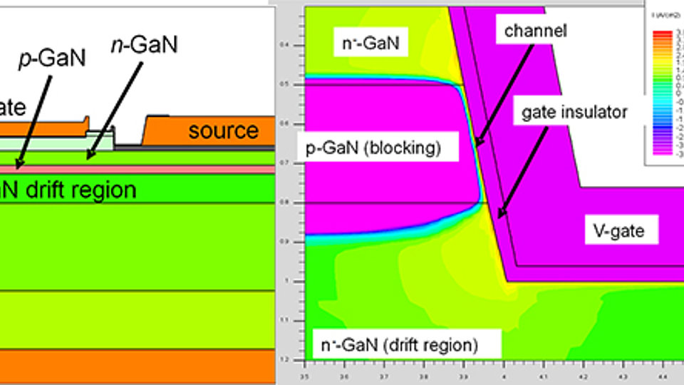
Fig. 1. (left) <i>n</i>-channel MISFET structure; (middle) physics-based simulation of channel current density of vertical GaN MISFET in ON-state conduction operation at Vds = +5 V and Vgs = +10 V; (right) SEM micrograph of manufactured circular GaN MISFET.
Recent progress in the development of low defect density free standing GaN substrates facilitates vertical GaN-based transistors for switching applications. This is a desired concept due to its reduced wafer ‘foot print A’, in comparison to lateral HFETs. It results in a reduction of RDS_ON × A by one order of magnitude down to ~1.0 mΩ∙cm2 and in reduced dispersion and switching losses. In addition, the possibility of strain-free homoepitaxy allows for growing thick n-GaN drift layers for OFF-state blocking capabilities exceeding 1 kV. At FBH, we have demonstrated a vertical n-channel MISFET grown by Metalorganic Vapor Phase Epitaxy on sapphire substrate. Circular MISFETs with 200 µm diameter were manufactured by defining a dry etched gate trench with 78° inclination down to the drain contact layer. An evaporated metal stack activated by rapid thermal annealing forms source and drain ohmic contacts. The gate insulator consists of a 20 nm thick Al2O3 layer formed by plasma-enhanced atomic layer deposition combined with in-situ NH3 plasma surface pretreatment. This process step has been performed in cooperation with SENTECH Instruments. The gate metal electrode consists of an electroplated 1 µm thick Au layer using TiW/Au as plating base.
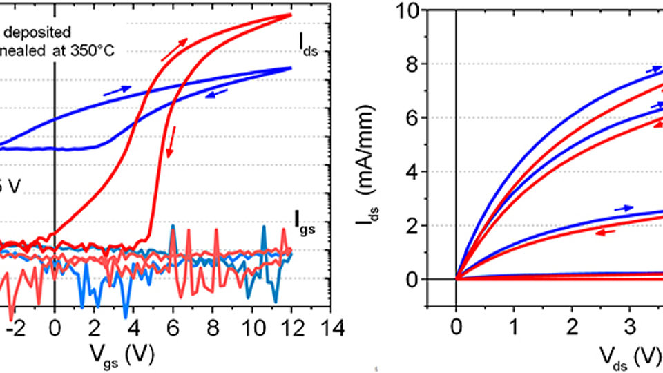
The devices are characterized immediately after the gate electrode formation and after annealing at 350°C for 45 min in N2 ambient. This post-metal-deposition annealing is an essential process step to prevent reliability degradation, to reduce mechanical stress in the metal-oxide interface and for recrystallizing the gate metal stack. When comparing the transistors’ transfer characteristics before and after the annealing step, it is observed that the on-state resistance reduces from ~13.6 kΩ∙mm to ~200 Ω∙mm, the on‑off ratio increased from 103 to 108, and Ids_max increases from ~0.2 mA/mm to ~20 mA/mm respectively (see Fig. 2, left). These are state-of-the-art results.
In conclusion, true vertical inversion type GaN MISFETs have been realized by combining high-quality GaN epitaxial growth of a vertical n-channel stack with a well-adapted vertical topology processing scheme and optimized high-quality Al2O3 PEALD gate insulator technology. The results demonstrate a promising technological baseline towards larger periphery vertical GaN MISFET devices for power electronics applications.
Support from the German BMBF and Investitionbank Berlin (ProFit project PioneerGaN, contract no. 10157776) is gratefully acknowledged.
Publications
E. Bahat Treidel, F. Naumann, H. Gargouri, O. Hilt, B. Martinez, J. Würfl, "Systematic Study on Plasma Enhanced Atomic Layer Deposited Al2O3 on n-GaN", as discussed at the 2016 IEEE SISC San Diego Ca. USA, Dec. 2016.
E. Bahat Treidel, O. Hilt, J. Stöver, V. Hoffmann, F. Brunner, K. Ickert, S. Hochheim, F. Naumann, H. Gargouri, B. Martinez, M. Weyers, J. Würfl, "GaN-based vertical n-channel MISFETs for switching applications", Proc. Compound Semiconductor Week (CSW), 14th - 18th May 2017, Berlin, Germany.

