Targeting 6G applications in the sub-THz range – advanced InP bipolar transistor process
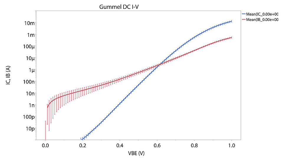
Fig. 2: Summary of Gummel plot performed on 42 sites on the wafer, demonstrating excellent yield (> 90 %) and low variation (below 5 %) across the wafer. Confirming the homogeneity of the newly developed TiW emitter process.
Fig. 3: Close-coupled 6” showerhead As/P MOCVD system at University of Duisburg-Essen (here shown in 6 x 2” wafer configuration).
InP bipolar transistor technology is perfectly suited for high-performance mm-wave and THz circuits, targeting 6G communication links operating in the range of 140 to 300 GHz. We develop the required technology in the Joint Lab cooperation between Ferdinand-Braun-Institut (FBH) and the University of Duisburg-Essen (UDE). Recently, epitaxial materials have been developed at UDE to facilitate such high frequency performance. Simultaneously, we have established a new and innovative process to down scale transistors at FBH. This allows harvesting the best performance of these epitaxial materials.
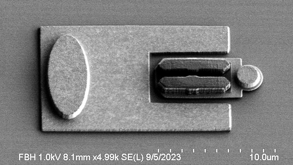
Deep sub-micron scaling of the critical transistor features enables higher transit and maximum oscillation frequency for a given epitaxial structure. New processing techniques have to be developed to accommodate such scaling requirements. Using electron beam lithography, we applied an etch-back based approach for the emitter structuring process with TiW as emitter metal. The resulting emitters possess a high aspect ratio, making them favorable for the planarization process while maintaining high transistor yield. A fully processed transistor is depicted in Fig. 1. Measurements of these processed transistors show excellent yield (> 90 %) and low variation (below 5 %) across the wafer (see Fig. 2).
Epitaxial structures are developed in UDE’s closed-couple showerhead MOCVD reactor capable of growing up to 6” diameter wafers (funded by BMBF ForLab, Fig. 3). For THz sensing and high precision ranging, a THz source with phase control by injection locking could be demonstrated with high output power of > 0.5 mW and close to 2 % conversion efficiency, operating at 420 GHz [1]. To scale InP HBT further down and enable improved THz performance, the series resistances in base and emitter need to be reduced. They are the cause for degrading device performance due to RC delay terms. Carbon p-doped InGaAs base layers, lattice matched to InP, could be realized at reduced growth temperatures. In hydride-free metalorganic growth, 1.8E19 cm-3 hole concentration and a sheet resistance around 1200 Ω/sq could be obtained so far for 30 nm thick layers. The emitter contact is formed on highly n-doped InGaAs on top of the epitaxial stack. Contact metal is deposited by electron beam evaporation in UDE’s dedicated metallization system, which includes a nitrogen-purged preparation chamber, resulting in ultra-clean metal-semiconductor interfaces. With 1.9E19 cm-3 electron concentration, an n-contact resistance of less than 4 Ωµm² was measured. This translates to less than 3 Ω emitter resistance for 250 nm emitter width and 6 µm emitter length, needed for 700 GHz transistors which are currently being developed.
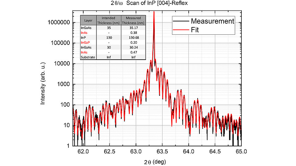
A sharp InP/InGaAs interface at the emitter-base heterojunction is important for high electron injection efficiency. X-ray modeling of the heterointerface describes an interlayer thickness of 0.5 nm, thus atomically sharp interfaces could be achieved This is shown in Fig. 4 in a typical base-emitter structure. The interface quality was confirmed by repeated epitaxy of 10 nm thick InGaAs quantum wells embedded in InP barriers. The structures exhibited photoluminescence spectra with FWHM of less than 15 meV when measured at 12 K. We further confirmed repeatability over multiple growth runs and ~1% homogeneity on 3” wafers in high resolution X-ray diffraction wafer maps.
These activities have been funded by the German Federal Ministry of Education and Research (BMBF) within the frameworks of “Forschungslabore Mikroelektronik Deutschland (ForLab) – Research Laboratories Microelectronics Germany”and Research Fab Microelectronics Germany (FMD).
Publication
[1] A. Possberg, F. Vogelsang, N. Pohl, M. Hossain, H. Yacoub, T. K. Johansen, W. Heinrich, and N. Weimann, “An Injection-Lockable InP-DHBT Source Operating at 421 GHz with −2.4 dBm Output Power and 1.7% DC-to-RF Efficiency,” in 2022 IEEE/MTT-S International Microwave Symposium - IMS 2022, Jun. 2022, pp. 336–339. doi: 10.1109/IMS37962.2022.9865468.


