Advancements in characterization techniques for high-speed transistors
Fig. 1: An example of a generic-probe-excitation model considering THRU calibration standard developed for electromagnetic simulations. The substrate is not shown for visualization.
Future wireless systems operating in the frequency range beyond 100 GHz will enable a multitude of applications, such as high data-rate communications, radar sensing, and imaging. Key components of these systems are high-speed transistors. At FBH, we develop Indium phosphide (InP) heterojunction bipolar transistors (HBTs), which are attractive candidates for these applications because they offer not only high speed but also high output power and efficiency.
One of the key performance metrics for transistors is the maximum frequency of oscillation. This is typically obtained from on-wafer measurements to avoid influences of, e.g., packaging, bonding, and interconnects. However, the maximum frequency of oscillation can only be determined with large uncertainties, due to unwanted effects introduced by instrumentation, probes, and electromagnetic coupling to neighboring structures. Therefore, accurate and reliable on-wafer characterization techniques are paramount for extracting this parameter, which is often used for comparison and benchmarking.
At FBH, we systematically investigate various factors to identify the sources of anomalies when extracting the maximum frequency of oscillation from measurements. We perform a full-wave 3D electromagnetic simulation by employing, e.g., a generic on-wafer probe model (see Fig. 1) using CST Studio Suite® to obtain the scattering parameters of the structures required for characterization.
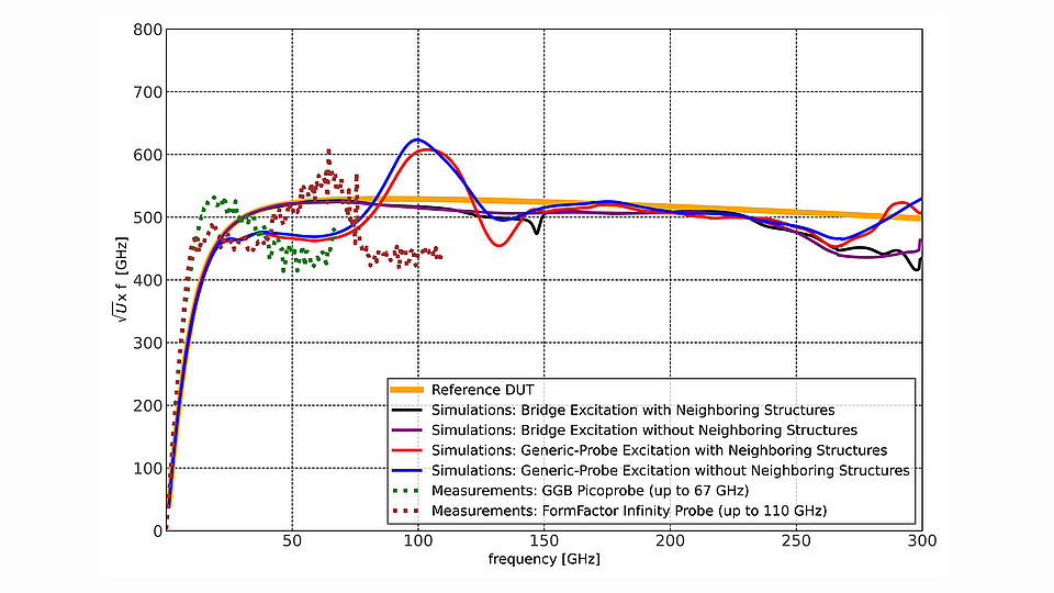
In addition to fabricating high-speed transistors using InP-HBT technology, FBH is capable of conducting on-wafer measurement up to 220 GHz. The square-root of the so-called unilateral gain multiplied by frequency is a common representation for the extraction of the maximum frequency of oscillation. Fig. 2 shows the extracted maximum frequency of oscillation for four simulation configurations and two measurement campaigns. Our investigations indicate that the anomalies observed in the maximum frequency of oscillation are very likely a result of on-wafer parasitic effects, especially probe-to-probe coupling, while the influence of neighboring structures is found to be negligible.
Under the recently started 23IND10 OnMicro project, we aim to employ more advanced calibration algorithms for characterizing InP HBTs. The advanced calibration algorithms account for probe-to-probe coupling by using dedicated new calibration structures. These special calibration structures are designed and simulated to assess the capabilities of the advanced calibration algorithm for transistor characterization. The simulation results show promising improvement in Mason’s gain behavior and reduced uncertainties in determining the maximum frequency of oscillation. The new calibration structures are already fabricated and currently being measured. It is expected that this data allows for accurate extraction of the maximum frequency of oscillation. The advanced calibration algorithms significantly enhance our capabilities in developing and characterizing high-speed InP-HBT-based devices for future high-frequency applications.
This work is supported in part by the Deutsche Forschungsgemeinschaft (DFG) under the grants FL 1201/1-1 and HE 1676/25-1. Also, this work is supported in part by the European Partnership on Metrology (EPM) project under the grant 23IND10 OnMicro. The 23IND10 OnMicro project is co-financed by European Union’s Horizon European Research and Innovation Program and by Participating States.
Publication
A. Kanitkar, R. Doerner, T. K. Johansen, W. Heinrich, and T. Flisgen, „Influence of On-Wafer Parasitic Effects on Mason’s Gain of Down-Scaled InP HBTs“, European Microwave Conference (EuMC) 2024 (accepted for publication).

