Lateral β-Ga2O3 MOSFET for power switching applications with a breakdown voltage of 1.8 kV
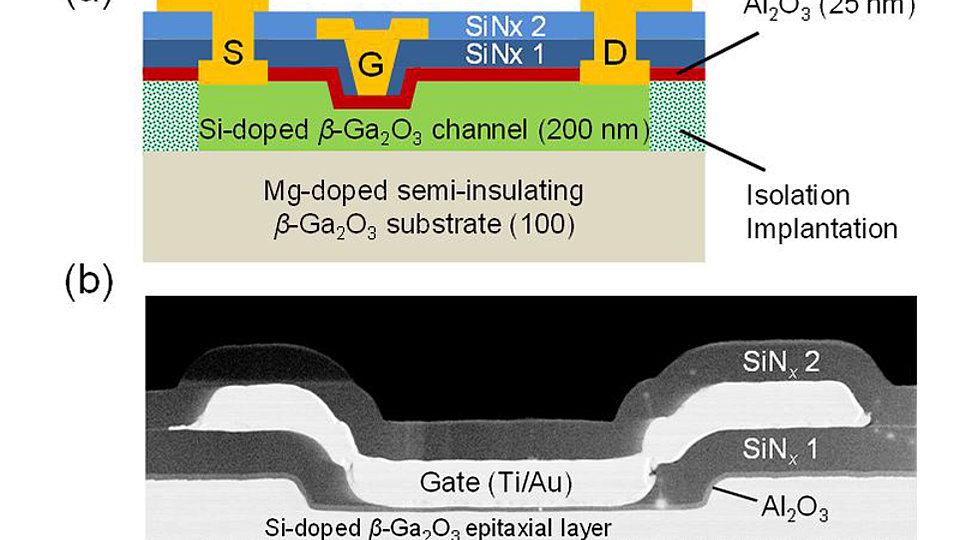
Fig. 1. Schematic cross-section of the β-Ga2O3 power transistor devices (a) and TEM image showing the recessed gate topology of the processed β-Ga2O3 power transistors (b).
Fig. 2. Transfer and output characteristics for fabricated β-Ga2O3 transistor devices with LGD of 2 µm (a), (b) and 10 µm (c), (d)
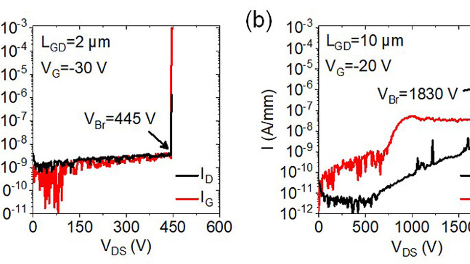
Fig. 3. Three terminal off-state breakdown measurements of β-Ga2O3 transistor devices with LGD of 2 µm (a) and 10 µm (b) showing catastrophic breakdown.
The ultra-wide bandgap semiconductor material β-Ga2O3 has drawn a lot of attention in recent years. Outstanding material properties make gallium oxide a promising candidate for next-generation power electronic applications. Taking its very high bandgap of 4.8 eV into account, an impressive material breakdown strength of 8 MV/cm is expected. This could pave the way for realizing high voltage switching devices with even higher power densities and efficiencies than it is currently possible using the SiC and GaN counterparts. So far, several studies have demonstrated the successful fabrication of power transistors based on β-Ga2O3; among them are reports showing record average field strength of 3.8 MV/cm as well as breakdown voltages up to 2.32 kV. However, the overall performances of those β-Ga2O3 devices are far away from the theoretical limit for β-Ga2O3. Up to now, the demonstrated power densities are still beneath the values for SiC or GaN devices and hover around the theoretical limit of Si-based devices. This is due to material and/or device related impairments.
In an attempt to overcome these issues FBH and IKZ have started to work on the fabrication of lateral β-Ga2O3-based power transistors with enhanced device performance through combining optimized layer growth and improved process technology. Optimization of the layer growth is mainly achieved by the homoepitaxial deposition of n-type β-Ga2O3 on vicinal surfaces. This results in layers with low defect densities and enhanced electrical properties, which facilitates low ON resistances. Moreover, a more advanced recessed T-gate topology has been implemented, allowing for electrical field reduction at the gate edge. Thus, it was possible to demonstrate transistor devices beyond the current state of the art, showing an enhanced breakdown voltage level and a high on-state conductivity at the same time.
The principal device structure of the fabricated β-Ga2O3 transistors is given in Fig. 1(a). All lateral structuring was done by i-line stepper lithography. The final devices featured gate-to-drain distances LGD of 2, 3, 4, 6, 8 and 10 µm at a fixed gate-to-source separation LGS of 1 µm as well as a gate length LG and width W of 700 nm and 250 µm, respectively. Fig. 1(b) shows the TEM cross-section of the gate topology of a fully processed transistor. Respective transfer and output curves for transistor devices with LGD of 2 µm and 10 µm are given in Fig. 2. The transfer characteristics demonstrate excellent on/off current ratios of more than 9 orders of magnitude. Due to the superior quality of the Al2O3, dielectric off-state current levels below 10-10 A/mm are achieved together with a negligible hysteresis of the transfer characteristics and subthreshold swings below 250 mV/dec. The maximum drain current ID (VDS = 10 V) is ranging between 49 mA/mm for devices with LGD = 10 µm and 120 mA/mm for devices with LGD = 2 µm and is still below saturation. The on-resistances (70 - 185 Ωmm, depending on LGD) were extracted from the output curves at VG = 10 V and at low drain bias. The contact resistance contributes with ~6 Ωmm for each contact. Furthermore, breakdown measurements were carried out and respective results for devices with LGD of 2 and 10 µm are given in Fig. 3. They show catastrophic breakdown at 445 V and 1830 V, respectively. Here, the recessed T-gate with the slanted SiNx sidewalls of the passivation opening has a tremendously positive impact in order to reduce high fields emerging at the gate edge towards the drain allowing for such high VBr. Due to the fact that a significant increase of the gate current is already visible at around 750 V for the device with LGD = 10 µm, the catastrophic breakdown can most probably be related to gate dielectric failure.
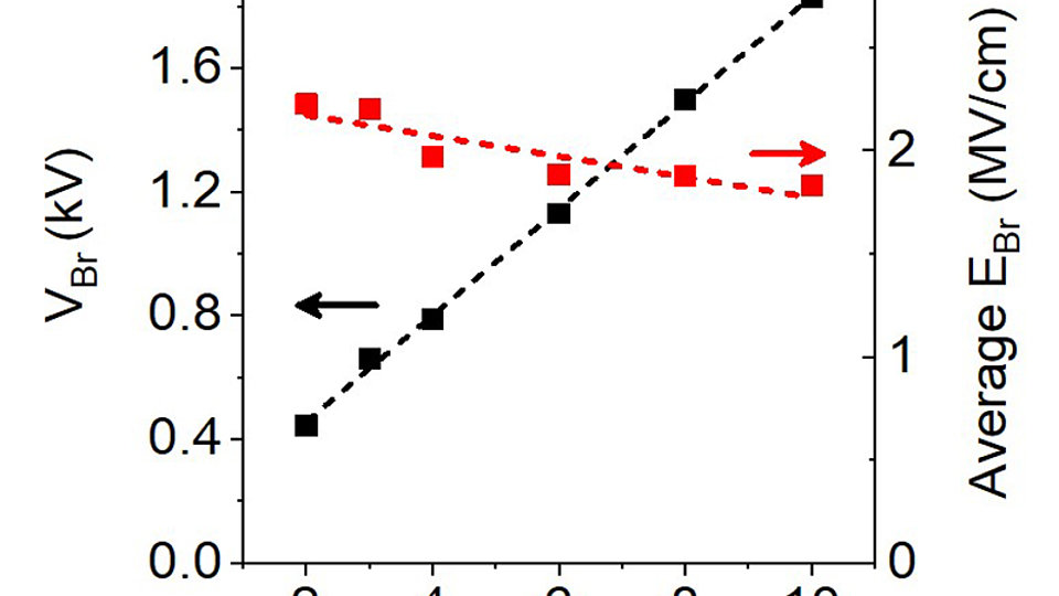
Fig. 4 depicts VBr as a function of LGD showing an almost linear relation. Additionally, the average breakdown field EBr only slightly decreases with increasing LGD. EBr ranges between 1.8 MV/cm and 2.2 MV/cm and is thus consistently higher as compared to other wide-bandgap devices like lateral GaN HFETs, vertical GaN transistors or SiC transistors which are well beneath 1.5 MV/cm. Using the specific ON resistance Ron,sp and VBr, it is possible to calculate the power figure of merit (PFOM = VBr2/Ron,sp), which is as high as 155 MW/cm2 for the transistor featuring a LGD of 10 µm. These results emphasize that combining the following technological aspects significantly improve β-Ga2O3 power transistor performance: high-resolution process technology using projection lithography, high quality Al2O3 gate insulator technology, optimized epitaxial layers with low defect density and high charge carrier density with enhanced electron mobility. With a more refined device optimization in terms of field plates and device passivation it is expected that the performance can be further pushed towards the theoretical limit of β-Ga2O3 power electronic devices.
Publications
[1] K. Tetzner, E. Bahat Treidel, O. Hilt, A. Popp, S. Bin Anooz, G. Wagner, A. Thies, K. Ickert, H. Gargouri, J. Würfl, ”Lateral 1.8 kV β-Ga2O3 MOSFET with 155 MW/cm2 power figure-of-merit” Electron Device Lett. (2019). doi: 10.1109/LED.2019.2930189
[2] O. Hilt, E. Bahat Treidel, M. Wolf, C. Kuring, K. Tetzner, H. Yazdani, A. Wentzel, J. Würfl, ”Lateral and vertical power transistors in GaN and Ga2O3” IET Power Electron., accepted and in press (2019). doi: 10.1049/iet-pel.2019.0059.
[3] K. Tetzner, A. Thies, E. Bahat Treidel, F. Brunner, G. Wagner, J. Würfl, “Selective area isolation of β-Ga2O3 using multiple energy nitrogen ion implantation,” Appl. Phys. Lett. 113, 172104 (2018). doi: 10.1063/1.5046139.


